
Datasheet


DocID022691 Rev 4 73/131
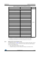
STM32F37xxx Electrical characteristics
114
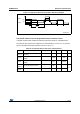
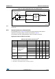
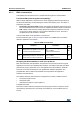
Figure 12. High-speed external clock source AC timing diagram
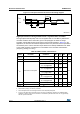
Low-speed external user clock generated from an external source
In bypass mode the LSE oscillator is switched off and the input pin is a standard GPIO.
The external clock signal has to respect the I/O characteristics in Section 6.3.14. However,
the recommended clock input waveform is shown in Figure 13.
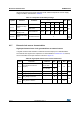
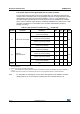
Table 39. Low-speed external user clock characteristics
Symbol Parameter
(1)
1. Guaranteed by design, not tested in production.
Conditions Min Typ Max Unit
f
LSE_ext
User External clock source
frequency
- 32.768 1000 kHz
V
LSEH
OSC32_IN input pin high level
voltage
0.7V
DD
-V
DD
V
V
LSEL
OSC32_IN input pin low level
voltage
V
SS
-0.3V
DD
t
w(LSEH)
t
w(LSEL)
OSC32_IN high or low time 450 - -
ns
t
r(LSE)
t
f(LSE)
OSC32_IN rise or fall time - - 50
MS19214V2
V
HSEH
t
f(HSE)
90%
10%
T
HSE
t
t
r(HSE)
V
HSEL
t
W(HSEH)
t
W(HSEL)