
Datasheet


Electrical characteristics STM32F37xxx
72/131 DocID022691 Rev 4
All timings are derived from tests performed under ambient temperature and V
DD
supply
voltage conditions summarized in Table 22.
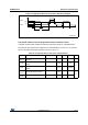
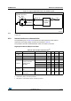
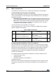
6.3.7 External clock source characteristics
High-speed external user clock generated from an external source
In bypass mode the HSE oscillator is switched off and the input pin is a standard GPIO.
The external clock signal has to respect the I/O characteristics in Section 6.3.14. However,
the recommended clock input waveform is shown in Figure 12.
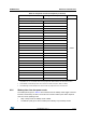
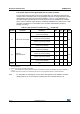
Table 37. Low-power mode wakeup timings
Symbol Parameter Conditions
Typ @V
DD
= V
DDA
Max Unit
= 2.0 V = 2.4 V = 2.7 V = 3 V = 3.3 V
t
WUSTOP
Wakeup from Stop
mode
Regulator in run mode 4.1 3.9 3.8 3.7 3.6 4.5
µs
Regulator in low
power mode
7.9 6.7 6.1 5.7 5.4 8.6
t
WUSTANDB
Y
Wakeup from
Standby mode
LSI and IWDG off 62.6 53.7 49.2 45.7 42.7 100
t
WUSLEEP
Wakeup from Sleep
mode
After WFE instruction 6
CPU
clock
cycles
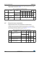
Table 38. High-speed external user clock characteristics
Symbol Parameter
(1)
1. Guaranteed by design, not tested in production.
Conditions Min Typ Max Unit
f
HSE_ext
User external clock source
frequency
CSS is on or
PLL is used
1
832MHz
CSS is off,
PLL not used
0
V
HSEH
OSC_IN input pin high level voltage 0.7 V
DD
V
DD
V
V
HSEL
OSC_IN input pin low level voltage V
SS
0.3 V
DD
t
w(HSEH)
t
w(HSEL)
OSC_IN high or low time 15 - -
ns
t
r(HSE)
t
f(HSE)
OSC_IN rise or fall time - - 20