
Datasheet

Electrical characteristics STM32F37xxx
68/131 DocID022691 Rev 4
I/O system current consumption
The current consumption of the I/O system has two components: static and dynamic.
I/O static current consumption
All the I/Os used as inputs with pull-up generate current consumption when the pin is
externally held low. The value of this current consumption can be simply computed by using
the pull-up/pull-down resistors values given in Table 52: I/O static characteristics.
For the output pins, any external pull-down or external load must also be considered to
estimate the current consumption.
Additional I/O current consumption is due to I/Os configured as inputs if an intermediate
voltage level is externally applied. This current consumption is caused by the input Schmitt
trigger circuits used to discriminate the input value. Unless this specific configuration is
required by the application, this supply current consumption can be avoided by configuring
these I/Os in analog mode. This is notably the case of ADC and SDADC input pins which
should be configured as analog inputs.
Caution: Any floating input pin can also settle to an intermediate voltage level or switch inadvertently,
as a result of external electromagnetic noise. To avoid current consumption related to
floating pins, they must either be configured in analog mode, or forced internally to a definite
digital value. This can be done either by using pull-up/down resistors or by configuring the
pins in output mode. Under reset conditions all I/Os are configured in input floating mode -
so if some inputs do not have a defined voltage level then they can generate additional
consumption. This consumption is visible on V
DD
supply and also on V
DDSDx
supply
because some I/Os are powered from SDADCx supply (all I/Os which have SDADC analog
input functionality).
I/O dynamic current consumption
In addition to the internal peripheral current consumption (see Table 36: Peripheral current
consumption), the I/Os used by an application also contribute to the current consumption.
When an I/O pin switches, it uses the current from the MCU supply voltage to supply the I/O
pin circuitry and to charge/discharge the capacitive load (internal or external) connected to
the pin:
where
I
SW
is the current sunk by a switching I/O to charge/discharge the capacitive load
V
DD
is the MCU supply voltage
f
SW
is the I/O switching frequency
C is the total capacitance seen by the I/O pin: C = C
INT
+ C
EXT
+ C
S
C
S
is the PCB board capacitance including the pad pin.
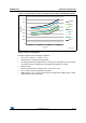
The test pin is configured in push-pull output mode and is toggled by software at a fixed
frequency.
I
SW
V
DD
f
SW
C××=