
Datasheet

DocID022691 Rev 4 63/131
STM32F37xxx Electrical characteristics
114
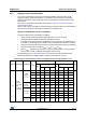
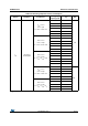
Note: V
DDA
monitoring is OFF and V
DDSD12
monitoring is OFF.
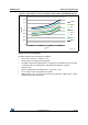
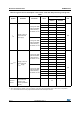
Table 29. Typical and maximum current consumption from V
DDA
supply
Symbol Parameter
Conditions
(1)
f
HCLK
V
DDA
= 2.4 V V
DDA
= 3.6 V
Unit
Typ
Max @ T
A
(2)
Typ
Max @ T
A
(2)
25 °C 85 °C 105 °C 25 °C 85 °C 105 °C
I
DDA
Supply
current in
Run or
Sleep
mode,
code
executing
from Flash
or RAM
HSE
bypass,
PLL on
72 MHz 228 261 274 280 249 288 304 311
µA
64 MHz 201 235 247 251 220 257 269 275
48 MHz 152 182 190 195 164 196 208 212
32 MHz 104 132 137 141 112 141 147 150
24 MHz 81 108 112 111 87 115 119 119
HSE
bypass,
PLL off
8 MHz 2 4 4 5 3 5 5 6
1 MHz 2 4 5 5 3 5 5 6
HSI clock,
PLL on
64 MHz 270 307 320 326 298 337 353 361
48 MHz 220 254 264 269 243 276 292 297
32 MHz 172 203 211 214 191 222 232 235
24 MHz 151 181 185 189 166 194 201 204
HSI clock,
PLL off
8 MHz 70 85 87 87 81 93 96 98
1. Current consumption from the V
DDA
supply is independent of whether the peripherals are on or off. Furthermore when the
PLL is off, I
DDA
is independent from the frequency.
2. Data based on characterization results, not tested in production unless otherwise specified.
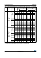
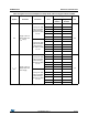
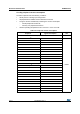
Table 30. Typical and maximum V
DD
consumption in Stop and Standby modes
Symbol Parameter Conditions
Typ@V
DD
(V
DD
=V
DDA
)Max
Unit
2.0 V 2.4 V 2.7 V 3.0 V 3.3 V 3.6 V
T
A
=
25 °C
T
A
=
85 °C
T
A
=
105 °C
I
DD
Supply
current in
Stop mode
Regulators in
run mode, all
oscillators
OFF
19.33 19.58 19.68 19.73 19.76 19.84 46.5 480 1019
µA
Regulators in
low-power
mode, all
oscillators
OFF
7.72 7.88 8.01 8.13 8.25 8.27 31.8 451.4 966.0
Supply
current in
Standby
mode
LSI ON and
IWDG ON
0.78 0.95 1.07 1.21 1.32 1.45 - - -
LSI OFF and
IWDG OFF
0.61 0.72 0.81 0.90 0.98 1.08 2.7 3.5 5.3