
Datasheet

DocID022691 Rev 4 61/131
STM32F37xxx Electrical characteristics
114
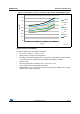
6.3.5 Supply current characteristics
The current consumption is a function of several parameters and factors such as the
operating voltage, ambient temperature, I/O pin loading, device software configuration,
operating frequencies, I/O pin switching rate, program location in memory and executed
binary code.
The current consumption is measured as described in Figure 10: Current consumption
measurement scheme.
All Run-mode current consumption measurements given in this section are performed with a
reduced code that gives a consumption equivalent to CoreMark code.
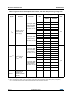
Typical and maximum current consumption
The MCU is placed under the following conditions:
• All I/O pins are in input mode with a static value at V
DD
or V
SS
(no load)
• All peripherals are disabled except when explicitly mentioned
• The Flash memory access time is adjusted to the f
HCLK
frequency (0 wait state from 0
to 24 MHz, 1 wait state from 24 to 48 MHz and 2 wait states from 48 MHz to 72 MHz)
• Prefetch in ON (reminder: this bit must be set before clock setting and bus prescaling)
• When the peripherals are enabled f
APB1
= f
AHB
/2 , f
APB2
= f
AHB
• When f
HCLK
> 8 MHz PLL is ON and PLL inputs is equal to HSI/2 = 4 MHz (if internal
clock is used) or HSE = 8 MHz (if HSE bypass mode is used)
The parameters given in Table 28 to Table 34 are derived from tests performed under
ambient temperature and supply voltage conditions summarized in Table 22.
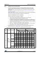
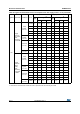
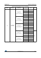
Table 28. Typical and maximum current consumption from V
DD
supply at V
DD
= 3.6 V
Symbol Parameter Conditions f
HCLK
All peripherals enabled All peripherals disabled
Unit
Typ
Max @ T
A
(1)
Typ
Max @ T
A
(1)
25 °C 85 °C 105 °C 25 °C 85 °C 105 °C
I
DD
Supply
current in
Run mode,
code
executing
from Flash
HSE
bypass,
PLL on
72 MHz 63.1 70.7 71.5 73.4 29.2 31.1 31.7 34.2
mA
64 MHz 56.3 63.3 64.1 64.9 26.1 27.8 28.4 30.4
48 MHz 42.5 48.5 48.0 50.1 19.9 22.6 21.9 23.1
32 MHz 28.8 31.4 32.2 34.3 13.1 16.1 14.9 16.2
24 MHz 21.9 24.4 24.4 25.8 10.1 10.9 11.9 12.4
HSE
bypass,
PLL off
8 MHz 7.3 8.0 9.3 9.3 3.7 4.1 4.4 5.0
1 MHz 1.1 1.5 1.8 2.3 0.8 1.1 1.4 1.9
HSI clock,
PLL on
64 MHz 51.7 57.7 58.0 60.4 25.8 27.6 28.1 30.1
48 MHz 38.6 45.9 43.5 46.9 19.8 21.9 21.7 22.8
32 MHz 26.4 31.1 29.7 31.9 13.1 15.7 14.8 16.2
24 MHz 20.3 22.6 22.6 23.7 6.9 7.5 8.1 8.8
HSI clock,
PLL off
8 MHz 7.0 7.6 8.8 8.8 3.7 4.1 4.4 5.0