
Datasheet


Electrical characteristics STM32F37xxx
58/131 DocID022691 Rev 4
6.3.2 Operating conditions at power-up / power-down
The parameters given in Table 23 are derived from tests performed under the ambient
temperature condition summarized in Table 22.
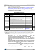
P
D
Power dissipation at T
A
= 85 °C
for suffix 6 or T
A
= 105 °C for
suffix 7
(4)
LQFP100 434
mW
LQFP64 444
LQFP48 364
BGA100 338
T
A
Ambient temperature for 6 suffix
version
Maximum power dissipation –40 85
°C
Low power dissipation
(5)
–40 105
Ambient temperature for 7 suffix
version
Maximum power dissipation –40 105
°C
Low power dissipation
(5)
–40 125
T
J Junction temperature range
6 suffix version –40 105
°C
7 suffix version –40 125
1. When the ADC is used, refer to Table 60: ADC characteristics.
2. To sustain a voltage higher than V
DD
+0.3 V, the internal pull-up/pull-down resistors must be disabled.
3. VDDSD12 is the external power supply for the PB2, PB10, and PE7 to PE15 I/O pins (the I/O pin ground is
internally connected to VSS). VDDSD3 is the external power supply for PB14 to PB15 and PD8 to PD15
I/O pins (the I/O pin ground is internally connected to VSS).
4. If T
A
is lower, higher P
D
values are allowed as long as T
J
does not exceed T
Jmax
.
5. In low power dissipation state, T
A
can be extended to this range as long as T
J
does not exceed T
Jmax
.
Table 22. General operating conditions (continued)
Symbol Parameter Conditions Min Max Unit
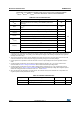
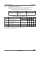
Table 23. Operating conditions at power-up / power-down
Symbol Parameter Conditions Min Max Unit
t
VDD
V
DD
rise time rate 0
∞
µs/V
V
DD
fall time rate 20 ∞
t
VDDA
V
DDA
rise time rate 0 ∞
V
DDA
fall time rate 20 ∞