
Datasheet


Electrical characteristics STM32F37xxx
56/131 DocID022691 Rev 4
Depending on the SDADCx operation mode, there can be more constraints between
V
REFSD+
, V
DDSD12
and V
DDSD3
which are described in reference manual RM0313.
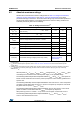
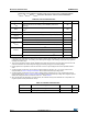
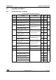
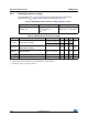
Table 20. Current characteristics
Symbol Ratings Max. Unit
ΣI
VDD
Total current into sum of all VDD_x
and VDDSDx power lines
(source)
(1)
160
mA
ΣI
VSS
Total current out of sum of all VSS_x
and VSSSD ground lines
(sink)
(1)
-160
I
VDD(PIN)
Maximum current into each VDD_x or VDDSDx power pin (source)
(1)
100
I
VSS(PIN)
Maximum current out of each VSS_x or VSSSD ground pin (sink)
(1)
-100
I
IO(PIN)
Output current sunk by any I/O and control pin 25
Output current source by any I/O and control pin -25
ΣI
IO(PIN)
Total output current sunk by sum of all IOs and control pins
(2)
80
Total output current sourced by sum of all IOs and control pins
(2)
-80
I
INJ(PIN)
Injected current on FT, FTf and B pins
(3)
-5/+0
Injected current on TC and RST pin
(4)
± 5
Injected current on TTa pins
(5)
± 5
ΣI
INJ(PIN)
Total injected current (sum of all I/O and control pins)
(6)
± 25
1. VDDSD12 is the external power supply for the PB2, PB10, and PE7 to PE15 I/O pins (the I/O pin ground is internally
connected to V
SS
). VDDSD3 is the external power supply for PB14 to PB15 and PD8 to PD15 I/O pins (the I/O pin ground
is internally connected to V
SS
). V
DD
(VDD_x) is the external power supply for all remaining I/O pins (the I/O pin ground is
internally connected to V
SS
).
2. This current consumption must be correctly distributed over all I/Os and control pins. The total output current must not be
sunk/sourced between two consecutive power supply pins referring to high pin count LQFP packages.
3. Positive injection is not possible on these I/Os and does not occur for input voltages lower than the specified maximum
value.
4. A positive injection is induced by V
IN
>V
DD
while a negative injection is induced by V
IN
< V
SS
. I
INJ(PIN)
must never be
exceeded. Refer to Table 19: Voltage characteristics for the maximum allowed input voltage values.
5. A positive injection is induced by V
IN
>V
DDA
while a negative injection is induced by V
IN
< V
SS
. I
INJ
(PIN) must never be
exceeded. Refer also to Table 19: Voltage characteristics for the maximum allowed input voltage values. Negative injection
disturbs the analog performance of the device. See note
(2)
below Tab le 62.
6. When several inputs are submitted to a current injection, the maximum ΣI
INJ(PIN)
is the absolute sum of the positive and
negative injected currents (instantaneous values).
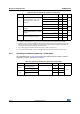
Table 21. Thermal characteristics
Symbol Ratings Value Unit
T
STG
Storage temperature range –65 to +150 °C
T
J
Maximum junction temperature 150 °C