
Datasheet


DocID022691 Rev 4 55/131
STM32F37xxx Electrical characteristics
114
6.2 Absolute maximum ratings
Stresses above the absolute maximum ratings listed in Table 19: Voltage characteristics,
Table 20: Current characteristics, and Table 21: Thermal characteristics may cause
permanent damage to the device. These are stress ratings only and functional operation of
the device at these conditions is not implied. Exposure to maximum rating conditions for
extended periods may affect device reliability.
All main power (V
DD
, V
DDSD12
, V
DDSD3
and V
DDA
) and ground (V
SS
, V
SSSD
, and V
SSA
) pins
must always be connected to the external power supply, in the permitted range.
The following relationship must be respected between V
DDA
and V
DD
: V
DDA
must power on
before or at the same time as V
DD
in the power up sequence. V
DDA
must be greater than or
equal to V
DD
.
The following relationship must be respected between V
DDA
and V
DDSD12
: V
DDA
must power
on before or at the same time as V
DDSD12
or V
DDSD3
in the power up sequence. V
DDA
must
be greater than or equal to V
DDSD12
or V
DDSD3
.
The following relationship must be respected between V
DDSD12
and V
DDSD3
: V
DDSD3
must
power on before or at the same time as V
DDSD12
in the power up sequence.
After power up (V
DDSD12
> Vrefint = 1.2 V) V
DDSD3
can be higher or lower than V
DDSD12
.
The following relationship must be respected between V
REFSD+
and V
DDSD12
, V
DDSD3
:
V
REFSD+
must be lower than V
DDSD3
.
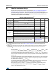
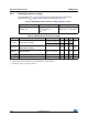
Table 19. Voltage characteristics
(1)
Symbol Ratings Min Max Unit
V
DD
–V
SS
External main supply voltage (including V
DDA,
V
DDSDx
,
V
BAT
and V
DD
)
− 0.3 4.0
V
V
DD
–V
DDA
Allowed voltage difference for V
DD
> V
DDA
-0.4
V
DDSDx
– V
DDA
Allowed voltage difference for V
DDSDx
> V
DDA
-0.4
V
REFSD+
–
V
DDSD3
Allowed voltage difference for V
REFSD+
> V
DDSD3
-0.4
V
REF+
– V
DDA
Allowed voltage difference for V
REF+
> V
DDA
-0.4
V
IN
(2)
Input voltage on FT and FTf pins V
SS
− 0.3 V
DD
+ 4.0
Input voltage on TTa pins V
SS
− 0.3 4.0
Input voltage on TC pins on SDADCx channels inputs
(3)
V
SS
− 0.3 4.0
Input voltage on any other pin V
SS
− 0.3 4.0
|V
SSX
− V
SS
| Variations between all the different ground pins 50 mV
V
ESD(HBM)
Electrostatic discharge voltage (human body model)
see Section 6.3.12:
Electrical sensitivity
characteristics
1. All main power (V
DD
, V
DDA
) and ground (V
SS
, V
SSA
) pins must always be connected to the external power supply, in the
permitted range.
2. V
IN
maximum must always be respected. Refer to Table 20: Current characteristics for the maximum allowed injected
current values.
3. VDDSD12 is the external power supply for PB2, PB10, and PE7 to PE15 I/O pins (I/O ground pin is internally connected to
V
SS
). VDDSD3 is the external power supply for PB14 to PB15 and PD8 to PD15 I/O pins (I/O ground pin is internally
connected to V
SS
).