
Datasheet


Electrical characteristics STM32F37xxx
52/131 DocID022691 Rev 4
6 Electrical characteristics
6.1 Parameter conditions
Unless otherwise specified, all voltages are referenced to V
SS
.
6.1.1 Minimum and maximum values
Unless otherwise specified, the minimum and maximum values are guaranteed in the worst
conditions of ambient temperature, supply voltage and frequencies by tests in production on
100% of the devices with an ambient temperature at T
A
= 25 °C and T
A
= T
A
max (given by
the selected temperature range).
Data based on characterization results, design simulation and/or technology characteristics
are indicated in the table footnotes and are not tested in production. Based on
characterization, the minimum and maximum values refer to sample tests and represent the
mean value plus or minus three times the standard deviation (mean±3σ).
6.1.2 Typical values
Unless otherwise specified, typical data are based on T
A
= 25 °C, V
DD
= V
DDA
= V
DDSDx
=
3.3 V. They are given only as design guidelines and are not tested.
Typical ADC and SDADC accuracy values are determined by characterization of a batch of
samples from a standard diffusion lot over the full temperature range, where 95% of the
devices have an error less than or equal to the value indicated
(mean±2σ).
6.1.3 Typical curves
Unless otherwise specified, all typical curves are given only as design guidelines and are
not tested.
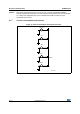
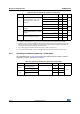
6.1.4 Loading capacitor
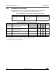
The loading conditions used for pin parameter measurement are shown in Figure 7.
6.1.5 Pin input voltage
The input voltage measurement on a pin of the device is described in Figure 8.
Figure 7. Pin loading conditions Figure 8. Pin input voltage
MS19210V1
C = 50 pF
MCU pin
MS19211V1
MCU pin
V
IN