
Datasheet

DocID022691 Rev 4 19/131
STM32F37xxx Functional overview
47
3.15 Fast comparators (COMP)
The STM32F373x embeds up to 2 comparators with rail-to-rail inputs and high-speed
output. The reference voltage can be internal or external (delivered by an I/O).
The threshold can be one of the following:
• DACs channel outputs
• External I/O
• Internal reference voltage (V
REFINT
) or submultiple (1/4 V
REFINT
, 1/2 V
REFINT
and 3/4
V
REFINT
)
The comparators can be combined into a window comparator.
Both comparators can wake up the device from Stop mode and generate interrupts and
breaks for the timers.
3.16 Touch sensing controller (TSC)
The devices provide a simple solution for adding capacitive sensing functionality to any
application. Capacitive sensing technology is able to detect the presence of a finger near an
electrode which is protected from direct touch by a dielectric (glass, plastic, ...). The
capacitive variation introduced by the finger (or any conductive object) is measured using a
proven implementation based on a surface charge transfer acquisition principle. It consists
of charging the electrode capacitance and then transferring a part of the accumulated
charges into a sampling capacitor until the voltage across this capacitor has reached a
specific threshold. To limit the CPU bandwidth usage this acquisition is directly managed by
the hardware touch sensing controller and only requires few external components to
operate.
The touch sensing controller is fully supported by the STMTouch touch sensing firmware
library, which is free to use and allows touch sensing functionality to be implemented reliably
in the end application.
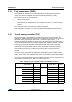
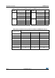
Up to 24 touch sensing electrodes can be controlled by the TSC. The touch sensing I/Os are
organized in 8 acquisition groups, with up to 4 I/Os in each group.
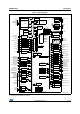
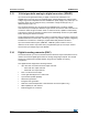
Table 3. Capacitive sensing GPIOs available on STM32F373x devices
Group
Capacitive sensing
signal name
Pin name Group
Capacitive sensing
signal name
Pin
name
1
TSC_G1_IO1 PA0
5
TSC_G5_IO1 PB3
TSC_G1_IO2 PA1 TSC_G5_IO2 PB4
TSC_G1_IO3 PA2 TSC_G5_IO3 PB6
TSC_G1_IO4 PA3 TSC_G5_IO4 PB7
2
TSC_G2_IO1 PA4
6
TSC_G6_IO1 PB14
TSC_G2_IO2 PA5 TSC_G6_IO2 PB15
TSC_G2_IO3 PA6 TSC_G6_IO3 PD8
TSC_G2_IO4 PA7 TSC_G6_IO4 PD9