
Datasheet

DocID022691 Rev 4 105/131
STM32F37xxx Electrical characteristics
114
6.3.21 V
BAT
monitoring characteristics
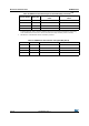
6.3.22 Timer characteristics
The parameters given in Table 68 are guaranteed by design.
Refer to Section 6.3.14: I/O port characteristics for details on the input/output alternate
function characteristics (output compare, input capture, external clock, PWM output).
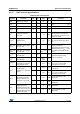
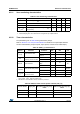
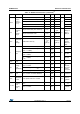
Table 67. V
BAT
monitoring characteristics
Symbol Parameter Min Typ Max Unit
R Resistor bridge for V
BAT
-50-KΩ
Q Ratio on V
BAT
measurement - 2 -
Er
(1)
1. Guaranteed by design, not tested in production.
Error on Q -1 - +1 %
T
S_vbat
(2)
2. Shortest sampling time can be determined in the application by multiple iterations.
ADC sampling time when reading the V
BAT
1mV accuracy
5--µs
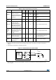
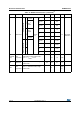
Table 68. TIMx
(1)
(2)
characteristics
1. TIMx is used as a general term to refer to the TIM2, TIM3, TIM4, TIM5, TIM6, TIM7, TIM12, TIM13, TIM14,
TIM15, TIM16 , TIM17, TIM18 and TIM19 timers.
2. Data based on characterization results, not tested in production.
Symbol Parameter Conditions Min Max Unit
t
res(TIM)
Timer resolution time
1-t
TIMxCLK
f
TIMxCLK
= 72 MHz 13.9 - ns
f
EXT
Timer external clock
frequency on CH1 to CH4
0f
TIMxCLK
/2 MHz
f
TIMxCLK
= 72 MHz 0 24 MHz
Res
TIM
Timer resolution
TIMx (except
TIM2)
-16
bit
TIM2 - 32
t
COUNTER
16-bit counter clock period
1 65536 t
TIMxCLK
f
TIMxCLK
= 72 MHz 0.0139 910 µs
t
MAX_COUN
T
Maximum possible count
with 32-bit counter
- 65536 × 65536 t
TIMxCLK
f
TIMxCLK
= 72 MHz - 59.65 s
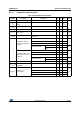
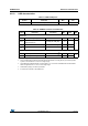
Table 69. IWDG min/max timeout period at 40 kHz (LSI)
(1)(2)
Prescaler divider PR[2:0] bits
Min timeout (ms) RL[11:0]=
0x000
Max timeout (ms) RL[11:0]=
0xFFF
/4 0 0.1 409.6
/8 1 0.2 819.2
/16 2 0.4 1638.4