
Datasheet


Electrical characteristics STM32F303xB STM32F303xC
102/133 DocID023353 Rev 7
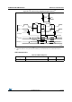
Figure 30. USB timings: definition of data signal rise and fall time
Table 64. USB DC electrical characteristics
Symbol Parameter Conditions Min.
(1)
1. All the voltages are measured from the local ground potential.
Max.
(1)
Unit
Input levels
V
DD
USB operating voltage
(2)
2. To be compliant with the USB 2.0 full-speed electrical specification, the USB_DP (D+) pin should be pulled
up with a 1.5 k resistor to a 3.0-to-3.6 V voltage range.
3.0
(3)
3. The STM32F303xB/STM32F303xC USB functionality is ensured down to 2.7 V but not the full USB
electrical characteristics which are degraded in the 2.7-to-3.0 V V
DD
voltage range.
3.6 V
V
DI
(4)
4. Guaranteed by design, not tested in production.
Differential input sensitivity I(USB_DP, USB_DM) 0.2 -
VV
CM
(4)
Differential common mode range Includes V
DI
range 0.8 2.5
V
SE
(4)
Single ended receiver threshold 1.3 2.0
Output levels
V
OL
Static output level low R
L
of 1.5 k to 3.6 V
(5)
5.
R
L
is the load connected on the USB drivers.
-0.3
V
V
OH
Static output level high R
L
of 15 k to V
SS
(5)
2.8 3.6
ai14137
t
f
Differen tial
Data L ines
V
SS
V
CR S
t
r
Crossover
points