
Datasheet


Electrical characteristics STM32F21xxx
66/175 DocID17050 Rev 9
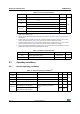
6.1.6 Power supply scheme
Figure 17. Power supply scheme
1. Each power supply pair must be decoupled with filtering ceramic capacitors as shown above. These capacitors must be
placed as close as possible to, or below, the appropriate pins on the underside of the PCB to ensure the good functionality
of the device.
2. To connect REGOFF pin, refer to Section 3.16: Voltage regulator.
3. The two 2.2 µF ceramic capacitors should be replaced by two 100 nF decoupling capacitors when the voltage regulator is
OFF.
4. The 4.7 µF ceramic capacitor must be connected to one of the V
DD
pin.
MS19041V2
V
DD
1/2/...14/15
Analog:
RCs, PLL,
...
Power switch
V
BAT
GP I/O s
OUT
IN
Kernel logic
(CPU,
digital
& RAM)
Backup circuitry
(OSC32K,RTC,
Backup registers,
backup RAM)
Wakeup logic
15 × 100 nF
+ 1 × 4.7 μF
1.8-3.6 V
Voltage
regulator
V
SS
1/2/...14/15
V
DDA
V
REF+
V
REF-
V
SSA
ADC
Level shifter
IO
Logic
V
DD
100 nF
+ 1 μF
V
REF
100 nF
+ 1 μF
V
DD
Flash memory
V
CAP_1
V
CAP_2
2 × 2.2 μF
REGOFF