
Datasheet


Electrical characteristics STM32F21xxx
134/175 DocID17050 Rev 9
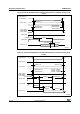
Synchronous waveforms and timings
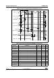
Figure 58 through Figure 61 represent synchronous waveforms and Table 76 through
Table 78 provide the corresponding timings. The results shown in these tables are obtained
with the following FSMC configuration:
• BurstAccessMode = FSMC_BurstAccessMode_Enable;
• MemoryType = FSMC_MemoryType_CRAM;
• WriteBurst = FSMC_WriteBurst_Enable;
• CLKDivision = 1; (0 is not supported, see the STM32F20xxx/21xxx reference manual)
• DataLatency = 1 for NOR Flash; DataLatency = 0 for PSRAM
In all timing tables, the
T
HCLK
is the HCLK clock period.
Figure 58. Synchronous multiplexed NOR/PSRAM read timings
FSMC_CLK
FSMC_NEx
FSMC_NADV
FSMC_A[25:16]
FSMC_NOE
FSMC_AD[15:0]
AD[15:0] D1 D2
FSMC_NWAIT
(WAITCFG = 1b, WAITPOL + 0b)
FSMC_NWAIT
(WAITCFG = 0b, WAITPOL + 0b)
t
w(CLK)
t
w(CLK)
Data latency = 0
BUSTURN = 0
t
d(CLKL-NExL)
t
d(CLKL-NExH)
t
d(CLKL-NADVL)
t
d(CLKL-AV)
t
d(CLKL-NADVH)
t
d(CLKL-AIV)
t
d(CLKH-NOEL)
t
d(CLKL-NOEH)
t
d(CLKL-ADV)
t
d(CLKL-ADIV)
t
su(ADV-CLKH)
t
h(CLKH-ADV)
t
su(ADV-CLKH)
t
h(CLKH-ADV)
t
su(NWAITV-CLKH)
t
h(CLKH-NWAITV)
t
su(NWAITV-CLKH)
t
h(CLKH-NWAITV)
t
su(NWAITV-CLKH)
t
h(CLKH-NWAITV)
ai14893h