
Datasheet


Electrical characteristics STM32F21xxx
126/175 DocID17050 Rev 9
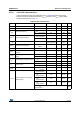
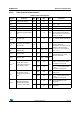
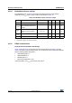
INL
(3)
Integral non linearity
(difference between
measured value at Code i
and the value at Code i on a
line drawn between Code 0
and last Code 1023)
-- ±1 LSB
Given for the DAC in 10-bit
configuration.
-- ±4 LSB
Given for the DAC in 12-bit
configuration.
Offset
(3)
Offset error
(difference between
measured value at Code
(0x800) and the ideal value =
V
REF+
/2)
-- ±10 mV
-- ±3 LSB
Given for the DAC in 10-bit at
V
REF+
= 3.6 V
-- ±12LSB
Given for the DAC in 12-bit at
V
REF+
= 3.6 V
Gain
error
(3)
Gain error - - ±0.5 %
Given for the DAC in 12-bit
configuration
t
SETTLING
(3)
Settling time (full scale: for a
10-bit input code transition
between the lowest and the
highest input codes when
DAC_OUT reaches final
value ±4LSB
-3 6 µs
C
LOAD
≤ 50 pF,
R
LOAD
≥ 5 kΩ
THD
(3)
Total Harmonic Distortion
Buffer ON
-- - dB
C
LOAD
≤ 50 pF,
R
LOAD
≥ 5 kΩ
Update
rate
(1)
Max frequency for a correct
DAC_OUT change when
small variation in the input
code (from code i to i+1LSB)
-- 1 MS/s
C
LOAD
≤ 50 pF,
R
LOAD
≥ 5 kΩ
t
WAKEUP
(3)
Wakeup time from off state
(Setting the ENx bit in the
DAC Control register)
- 6.5 10 µs
C
LOAD
≤ 50 pF, R
LOAD
≥ 5 kΩ
input code between lowest and
highest possible ones.
PSRR+
(1)
Power supply rejection ratio
(to V
DDA
) (static DC
measurement)
- –67 –40 dB No R
LOAD
, C
LOAD
= 50 pF
1. Guaranteed by design, not tested in production.
2. The quiescent mode corresponds to a state where the DAC maintains a stable output level to ensure that no dynamic
consumption occurs.
3. Guaranteed by characterization, not tested in production.
Table 67. DAC characteristics (continued)
Symbol Parameter Min Typ Max Unit Comments