
Datasheet


DocID15818 Rev 11 121/178
STM32F20xxx Electrical characteristics
177
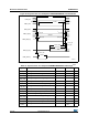
6.3.20 12-bit ADC characteristics
Unless otherwise specified, the parameters given in Table 66 are derived from tests
performed under the ambient temperature, f
PCLK2
frequency and V
DDA
supply voltage
conditions summarized in Table 14.
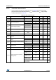
Table 66. ADC characteristics
Symbol Parameter Conditions Min Typ
Max Unit
V
DDA
Power supply 1.8
(1)
-3.6V
V
REF+
Positive reference voltage 1.8
(1)(2)
-V
DDA
V
f
ADC
ADC clock frequency
V
DDA
= 1.8
(1)
to 2.4 V 0.6 - 15 MHz
V
DDA
= 2.4 to 3.6 V 0.6 - 30 MHz
f
TRIG
(3)
External trigger frequency
f
ADC
= 30 MHz with
12-bit resolution
- - 1764 kHz
- - 17 1/f
ADC
V
AIN
Conversion voltage range
(4)
0 (V
SSA
or V
REF-
tied to ground)
-V
REF+
V
R
AIN
(3)
External input impedance
See Equation 1 for
details
--50kΩ
R
ADC
(3)(5)
Sampling switch resistance 1.5 - 6 kΩ
C
ADC
(3)
Internal sample and hold
capacitor
-4-pF
t
lat
(3)
Injection trigger conversion
latency
f
ADC
= 30 MHz - - 0.100 µs
--3
(6)
1/f
ADC
t
latr
(3)
Regular trigger conversion latency
f
ADC
= 30 MHz - - 0.067 µs
--2
(6)
1/f
ADC
t
S
(3)
Sampling time
f
ADC
= 30 MHz 0.100 - 16 µs
3-4801/f
ADC
t
STAB
(3)
Power-up time - 2 3 µs
t
CONV
(3)
Total conversion time (including
sampling time)
f
ADC
= 30 MHz
12-bit resolution
0.5 - 16.40 µs
f
ADC
= 30 MHz
10-bit resolution
0.43 - 16.34 µs
f
ADC
= 30 MHz
8-bit resolution
0.37 - 16.27 µs
f
ADC
= 30 MHz
6-bit resolution
0.3 - 16.20 µs
9 to 492 (t
S
for sampling +n-bit resolution for successive
approximation)
1/f
ADC