
Datasheet

Electrical characteristics STM32F20xxx
102/178 DocID15818 Rev 11
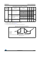
6.3.16 I/O port characteristics
General input/output characteristics
Unless otherwise specified, the parameters given in Table 50 are derived from tests
performed under the conditions summarized in Table 14: General operating conditions.
All I/Os are CMOS and TTL compliant except for BOOT0 and BOOT1.
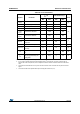
Table 46. I/O static characteristics
(1)
Symbol Parameter Conditions Min Typ Max Unit
V
IL
Low level
input voltage
TTa, FT and
NRST I/Os
1.6 V ≤ V
DD
≤ 3.6 V
- - 0.35V
DD
–0.04
(2)
V
BOOT0 - - TBD
(2)
I/O input low
level voltage
except BOOT0
- - 0.3V
DD
(3)
V
IH
High level
input voltage
TTa, FT and
NRST I/Os
(4)
0.45V
DD
+0.3
(2)
--
BOOT0 TBD
(2)
--
I/O input low
level voltage
except BOOT0
0.7V
DD
(3)
--
V
hys
Schmitt
trigger
hysteresis
TTa, FT and
NRST I/Os
10% V
DDIO
(2)(5)
--
mV
BOOT0 TBD
(2)
--
I
lkg
I/O input leakage current
(6)
V
SS
≤ V
IN
≤ V
DD
--±1
µA
I/O FT input leakage current
(5)
V
IN
= 5V - - 3
R
PU
Weak pull-up
equivalent
resistor
(7)
All pins except
for PA10 and
PB12
V
IN
= V
SS
30 40 50
kΩ
PA10 and PB12 8 11 15
R
PD
Weak pull-
down
equivalent
resistor
All pins except
for PA10 and
PB12
V
IN
= V
DD
30 40 50
PA10 and PB12 8 11 15
C
IO
(2)
I/O pin
capacitance
5pF
1. TBD stands for “to be defined”.
2. Data based on design simulation only. Not tested in production.
3. Tested in production.
4. To sustain a voltage higher than V
DD
+0.3 V, the internal pull-up/pull-down resistors must be disabled.
5. With a minimum of 200 mV.
6. Leakage could be higher than the maximum value, if negative current is injected on adjacent pins.
7. Pull-up and pull-down resistors are designed with a true resistance in series with a switchable PMOS/NMOS. This
MOS/NMOS contribution
to the series resistance is minimum (~10% order).