
Datasheet


Electrical characteristics STM32F20xxx
76/178 DocID15818 Rev 11
Typical and maximum current consumption
The MCU is placed under the following conditions:
• At startup, all I/O pins are configured as analog inputs by firmware.
• All peripherals are disabled except if it is explicitly mentioned.
• The
Flash memory access time is adjusted to f
HCLK
frequency (0 wait state from 0 to
30 MHz, 1 wait state from 30 to 60 MHz, 2 wait states from 60 to 90 MHz and 3 wait
states from 90 to 120 MHz).
• When the peripherals are enabled HCLK is the system clock, f
PCLK1
= f
HCLK
/4, and
f
PCLK2
= f
HCLK
/2, except is explicitly mentioned.
• The maximum values are obtained for V
DD
= 3.6 V and maximum ambient temperature
(T
A
), and the typical values for T
A
= 25 °C and V
DD
= 3.3 V unless otherwise specified.
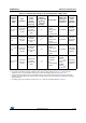
Table 20. Typical and maximum current consumption in Run mode, code with data processing
running from Flash memory (ART accelerator enabled) or RAM
(1)
Symbol Parameter Conditions f
HCLK
Typ Max
(2)
Unit
T
A
=
25 °C
T
A
=
85 °C
T
A
=
105 °C
I
DD
Supply current in
Run mode
External clock
(3)
, all
peripherals enabled
(4)
120 MHz 49 63 72
mA
90 MHz 38 51 61
60 MHz 26 39 49
30 MHz 14 27 37
25 MHz 11 24 34
16 MHz
(5)
82130
8 MHz 5 17 27
4 MHz 3 16 26
2 MHz 2 15 25
External clock
(3)
, all
peripherals disabled
120 MHz 21 34 44
90 MHz 17 30 40
60 MHz 12 25 35
30 MHz 7 20 30
25 MHz 5 18 28
16 MHz
(5)
4.0 17.0 27.0
8 MHz 2.5 15.5 25.5
4 MHz 2.0 14.7 24.8
2 MHz 1.6 14.5 24.6
1. Code and data processing running from SRAM1 using boot pins.
2. Based on characterization, tested in production at V
DD
max and f
HCLK
max with peripherals enabled.
3. External clock is 4 MHz and PLL is on when f
HCLK
> 25 MHz.
4. When the ADC is on (ADON bit set in the ADC_CR2 register), add an additional power consumption of 1.6 mA per ADC for
the analog part.
5. In this case HCLK = system clock/2.