
Datasheet


DocID15818 Rev 11 129/178
STM32F20xxx Electrical characteristics
177
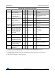
6.3.24 Embedded reference voltage
The parameters given in Table 71 are derived from tests performed under ambient
temperature and V
DD
supply voltage conditions summarized in Table 14.
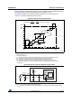
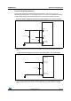
6.3.25 FSMC characteristics
Asynchronous waveforms and timings
Figure 56 through Figure 59 represent asynchronous waveforms and Table 72 through
Table 75 provide the corresponding timings. The results shown in these tables are obtained
with the following FSMC configuration:
• AddressSetupTime = 1
• AddressHoldTime = 1
• DataSetupTime = 1
• BusTurnAroundDuration = 0x0
In all timing tables, the
T
HCLK
is the HCLK clock period.
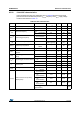
Table 71. Embedded internal reference voltage
Symbol Parameter Conditions Min
Typ
Max Unit
V
REFINT
Internal reference voltage –40 °C < T
A
< +105 °C 1.18 1.21 1.24 V
T
S_vrefint
(1)
1. Shortest sampling time can be determined in the application by multiple iterations.
ADC sampling time when
reading the internal reference
voltage
10 - - µs
V
RERINT_s
(2)
2. Guaranteed by design, not tested in production.
Internal reference voltage
spread over the temperature
range
V
DD
= 3 V - 3 5 mV
T
Coeff
(2)
Temperature coefficient - 30 50 ppm/°C
t
START
(2)
Startup time - 6 10 µs