
Datasheet

Electrical characteristics STM32F20xxx
86/178 DocID15818 Rev 11
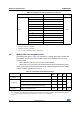
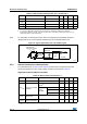
6.3.7 Wakeup time from low-power mode
The wakeup times given in Table 27 is measured on a wakeup phase with a 16 MHz HSI
RC oscillator. The clock source used to wake up the device depends from the current
operating mode:
• Stop or Standby mode: the clock source is the RC oscillator
• Sleep mode: the clock source is the clock that was set before entering Sleep mode.
All timings are derived from tests performed under ambient temperature and V
DD
supply
voltage conditions summarized in Table 14.
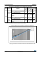
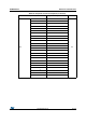
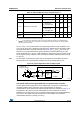
APB2
SDIO 0.69
mA
TIM1 1.06
TIM8 1.03
TIM9 0.58
TIM10 0.37
TIM11 0.39
ADC1
(4)
2.13
ADC2
(4)
2.04
ADC3
(4)
2.12
SPI1 1.20
USART1 0.38
USART6 0.37
1. External clock is 25 MHz (HSE oscillator with 25 MHz crystal) and PLL is on.
2. EN1 bit is set in DAC_CR register.
3. EN2 bit is set in DAC_CR register.
4. f
ADC
= f
PCLK2
/2, ADON bit set in ADC_CR2 register.
Table 26. Peripheral current consumption (continued)
Peripheral
(1)
Typical consumption at 25 °C Unit
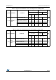
Table 27. Low-power mode wakeup timings
Symbol Parameter
Min
(1)
Typ
(1)
Max
(1)
Unit
t
WUSLEEP
(2)
Wakeup from Sleep mode - 1 - µs
t
WUSTOP
(2)
Wakeup from Stop mode (regulator in Run mode) - 13 -
µs
Wakeup from Stop mode (regulator in low power mode) - 17 40
Wakeup from Stop mode (regulator in low power mode
and Flash memory in Deep power down mode)
-110-
t
WUSTDBY
(2)(3)
Wakeup from Standby mode 260 375 480 µs
1. Based on characterization, not tested in production.
2. The wakeup times are measured from the wakeup event to the point in which the application code reads the first instruction.
3. t
WUSTDBY
minimum and maximum values are given at 105 °C and –45 °C, respectively.