
Datasheet

DocID15818 Rev 11 71/178
STM32F20xxx Electrical characteristics
177
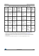
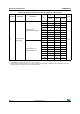
Table 15. Limitations depending on the operating power supply range
Operating
power
supply
range
ADC
operation
Maximum
Flash
memory
access
frequency
(f
Flashmax
)
Number of wait
states at
maximum CPU
frequency
(f
CPUmax
=
120 MHz)
(1)
I/O operation
FSMC_CLK
frequency for
synchronous
accesses
Possible
Flash
memory
operations
V
DD
=1.8 to
2.1 V
(2)
Conversion
time up to
1Msps
16 MHz with
no Flash
memory wait
state
7
(3)
– Degraded
speed
performance
– No I/O
compensation
up to 30 MHz
8-bit erase
and program
operations
only
V
DD
= 2.1 to
2.4 V
Conversion
time up to
1Msps
18 MHz with
no Flash
memory wait
state
6
(3)
– Degraded
speed
performance
– No I/O
compensation
up to 30 MHz
16-bit erase
and program
operations
V
DD
= 2.4 to
2.7 V
Conversion
time up to
2Msps
24 MHz with
no Flash
memory wait
state
4
(3)
– Degraded
speed
performance
–I/O
compensation
works
up to 48 MHz
16-bit erase
and program
operations
V
DD
= 2.7 to
3.6 V
(4)
Conversion
time up to
2Msps
30 MHz with
no Flash
memory wait
state
3
(3)
– Full-speed
operation
–I/O
compensation
works
–up to
60 MHz
when V
DD
=
3.0 to 3.6 V
–up to
48 MHz
when V
DD
=
2.7 to 3.0 V
32-bit erase
and program
operations
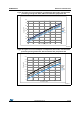
1. The number of wait states can be reduced by reducing the CPU frequency (see Figure 21).
2. On devices in WLCSP64+2 package, if IRROFF is set to V
DD
, the supply voltage can drop to 1.7 V when the device
operates in the 0 to 70 °C temperature range using an external power supply supervisor (see Section 3.16).
3. Thanks to the ART accelerator and the 128-bit Flash memory, the number of wait states given here does not impact the
execution speed from Flash memory since the ART accelerator allows to achieve a performance equivalent to 0 wait state
program execution.
4. The voltage range for OTG USB FS can drop down to 2.7 V. However it is degraded between 2.7 and 3 V.