
Datasheet

DocID15818 Rev 11 55/178
STM32F20xxx Pinouts and pin description
177
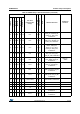
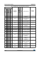
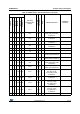
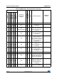
- - 98 142 170 A3 PE1 I/O FT
FSMC_NBL1, DCMI_D3,
EVENTOUT
-----D5 V
SS
S
63 D8 - - - - V
SS
S
- - 99 143 171 C6 RFU
(7)
64 D9 100 144 172 C5 V
DD
S
----173D4 PI4 I/OFT
TIM8_BKIN, DCMI_D5,
EVENTOUT
----174C4 PI5 I/OFT
TIM8_CH1, DCMI_VSYNC,
EVENTOUT
----175C3 PI6 I/OFT
TIM8_CH2, DCMI_D6,
EVENTOUT
----176C2 PI7 I/OFT
TIM8_CH3, DCMI_D7,
EVENTOUT
- C8 - - - - IRROFF I/O
1. Function availability depends on the chosen device.
2. PC13, PC14, PC15 and PI8 are supplied through the power switch. Since the switch only sinks a limited amount of current
(3 mA), the use of GPIOs PC13 to PC15 and PI8 in output mode is limited: the speed should not exceed 2 MHz with a
maximum load of 30 pF and these I/Os must not be used as a current source (e.g. to drive an LED).
3. Main function after the first backup domain power-up. Later on, it depends on the contents of the RTC registers even after
reset (because these registers are not reset by the main reset). For details on how to manage these I/Os, refer to the RTC
register description sections in the STM32F20x and STM32F21x reference manual, available from the STMicroelectronics
website: www.st.com.
4. FT = 5 V tolerant except when in analog mode or oscillator mode (for PC14, PC15, PH0 and PH1).
5. If the device is delivered in an UFBGA176 package and if the REGOFF pin is set to V
DD
(Regulator OFF), then PA0 is
used as an internal Reset (active low).
6. FSMC_NL pin is also named FSMC_NADV on memory devices.
7. RFU means “reserved for future use”. This pin can be tied to V
DD
,V
SS
or left unconnected.
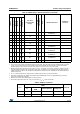
Table 8. STM32F20x pin and ball definitions (continued)
Pins
Pin name
(function after
reset)
(1)
Pin type
I/O structure
Note
Alternate functions
Additional
functions
LQFP64
WLCSP64+2
LQFP100
LQFP144
LQFP176
UFBGA176
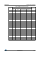
Table 9. FSMC pin definition
Pins
FSMC
LQFP100
CF
NOR/PSRAM/S
RAM
NOR/PSRAM Mux NAND 16 bit
PE2 A23 A23 Yes
PE3 A19 A19 Yes