
Datasheet


Functional overview STM32F20xxx
22/178 DocID15818 Rev 11
3.11 External interrupt/event controller (EXTI)
The external interrupt/event controller consists of 23 edge-detector lines used to generate
interrupt/event requests. Each line can be independently configured to select the trigger
event (rising edge, falling edge, both) and can be masked independently. A pending register
maintains the status of the interrupt requests. The EXTI can detect an external line with a
pulse width shorter than the Internal APB2 clock period. Up to 140 GPIOs can be connected
to the 16 external interrupt lines.
3.12 Clocks and startup
On reset the 16 MHz internal RC oscillator is selected as the default CPU clock. The
16 MHz internal RC oscillator is factory-trimmed to offer 1% accuracy. The application can
then select as system clock either the RC oscillator or an external 4-26 MHz clock source.
This clock is monitored for failure. If failure is detected, the system automatically switches
back to the internal RC oscillator and a software interrupt is generated (if enabled). Similarly,
full interrupt management of the PLL clock entry is available when necessary (for example if
an indirectly used external oscillator fails).
The advanced clock controller clocks the core and all peripherals using a single crystal or
oscillator. In particular, the ethernet and USB OTG FS peripherals can be clocked by the
system clock.
Several prescalers and PLLs allow the configuration of the three AHB buses, the high-
speed APB (APB2) and the low-speed APB (APB1) domains. The maximum frequency of
the three AHB buses is 120 MHz and the maximum frequency the high-speed APB domains
is 60 MHz. The maximum allowed frequency of the low-speed APB domain is 30 MHz.
The devices embed a dedicate PLL (PLLI2S) which allow to achieve audio class
performance. In this case, the I
2
S master clock can generate all standard sampling
frequencies from 8 kHz to 192 kHz.
3.13 Boot modes
At startup, boot pins are used to select one out of three boot options:
• Boot from user Flash
• Boot from system memory
• Boot from embedded SRAM
The boot loader is located in system memory. It is used to reprogram the Flash memory by
using USART1 (PA9/PA10), USART3 (PC10/PC11 or PB10/PB11), CAN2 (PB5/PB13), USB
OTG FS in Device mode (PA11/PA12) through DFU (device firmware upgrade).
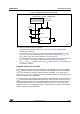
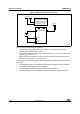
3.14 Power supply schemes
• V
DD
= 1.8 to 3.6 V: external power supply for I/Os and the internal regulator (when
enabled), provided externally through V
DD
pins. On devices in WLCSP64+2 package, if
IRROFF is set to V
DD
, the supply voltage can drop to 1.7 V when the device operates