
Datasheet

Electrical characteristics STM32F20xxx
148/178 DocID15818 Rev 11
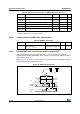
6.3.26 Camera interface (DCMI) timing specifications
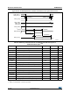
6.3.27 SD/SDIO MMC card host interface (SDIO) characteristics
Unless otherwise specified, the parameters given in Table 85 are derived from tests
performed under ambient temperature, f
PCLKx
frequency and V
DD
supply voltage conditions
summarized in Table 14.
Refer to Section 6.3.16: I/O port characteristics for more details on the input/output alternate
function characteristics (D[7:0], CMD, CK).
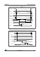
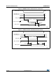
Figure 74. SDIO high-speed mode
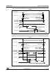
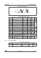
Table 83. Switching characteristics for NAND Flash write cycles
(1)(2)
1. C
L
= 30 pF.
2. Based on characterization, not tested in production.
Symbol Parameter Min Max Unit
t
w(NWE)
FSMC_NWE low width 4T
HCLK
- 1 4T
HCLK
+ 3 ns
t
v(NWE-D)
FSMC_NWE low to FSMC_D[15-0] valid - 0 ns
t
h(NWE-D)
FSMC_NWE high to FSMC_D[15-0] invalid 3T
HCLK
-ns
t
d(D-NWE)
FSMC_D[15-0] valid before FSMC_NWE high 5T
HCLK
-ns
t
d(ALE-NWE)
FSMC_ALE valid before FSMC_NWE low - 3T
HCLK
+ 2 ns
t
h(NWE-ALE)
FSMC_NWE high to FSMC_ALE invalid 3T
HCLK
- 2 - ns
Table 84. DCMI characteristics
Symbol Parameter Conditions Min Max
-
Frequency ratio
DCMI_PIXCLK/
f
HCLK
DCMI_PIXCLK= 48 MHz 0.4
t
W(CKH)
CK
D, CMD
(output)
D, CMD
(input)
t
C
t
W(CKL)
t
OV
t
OH
t
ISU
t
IH
t
f
t
r
ai14887