
Datasheet


Electrical characteristics STM32F20xxx
122/178 DocID15818 Rev 11
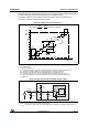
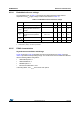
Equation 1: R
AIN
max formula
The formula above (Equation 1) is used to determine the maximum external impedance
allowed for an error below 1/4 of LSB. N = 12 (from 12-bit resolution) and k is the number of
sampling periods defined in the ADC_SMPR1 register.
a
Note: ADC accuracy vs. negative injection current: injecting a negative current on any analog
input pins should be avoided as this significantly reduces the accuracy of the conversion
f
S
(3)
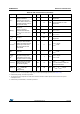
Sampling rate
(f
ADC
= 30 MHz)
12-bit resolution
Single ADC
- - 2 Msps
12-bit resolution
Interleave Dual ADC
mode
--3.75Msps
12-bit resolution
Interleave Triple ADC
mode
- - 6 Msps
I
VREF+
(3)
ADC V
REF
DC current
consumption in conversion mode
-300500µA
I
VDDA
(3)
ADC VDDA DC current
consumption in conversion mode
-1.61.8mA
1. On devices in WLCSP64+2 package, if IRROFF is set to V
DD
, the supply voltage can drop to 1.7 V when the device
operates in the 0 to 70 °C temperature range using an external power supply supervisor (see Section 3.16).
2. It is recommended to maintain the voltage difference between V
REF+
and V
DDA
below 1.8 V.
3. Based on characterization, not tested in production.
4. V
REF+
is internally connected to V
DDA
and V
REF-
is internally connected to V
SSA
.
5. R
ADC
maximum value is given for V
DD
=1.8 V, and minimum value for V
DD
=3.3 V.
6. For external triggers, a delay of 1/f
PCLK2
must be added to the latency specified in Table 66.
Table 66. ADC characteristics (continued)
Symbol Parameter Conditions Min Typ
Max Unit
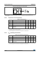
Table 67. ADC accuracy
(1)
1. Better performance could be achieved in restricted V
DD
, frequency and temperature ranges.
Symbol Parameter Test conditions Typ Max
(2)
2. Based on characterization, not tested in production.
Unit
ET Total unadjusted error
f
PCLK2
= 60 MHz,
f
ADC
= 30 MHz, R
AIN
< 10 kΩ,
V
DDA
= 1.8
(3)
to 3.6 V
3. On devices in WLCSP64+2 package, if IRROFF is set to V
DD
, the supply voltage can drop to 1.7 V when
the device operates in the 0 to 70 °C temperature range using an external power supply supervisor (see
Section 3.16).
±2 ±5
LSB
EO Offset error ±1.5 ±2.5
EG Gain error ±1.5 ±3
ED Differential linearity error ±1 ±2
EL Integral linearity error ±1.5 ±3
R
AIN
k0.5–()
f
ADC
C
ADC
2
N 2+
()ln××
-------------------------------------------------------------- R
ADC
–=