
Datasheet

Electrical characteristics STM32F20xxx
106/178 DocID15818 Rev 11
6.3.17 NRST pin characteristics
The NRST pin input driver uses CMOS technology. It is connected to a permanent pull-up
resistor, R
PU
(see Table 49).
Unless otherwise specified, the parameters given in Table 49 are derived from tests
performed under the ambient temperature and V
DD
supply voltage conditions summarized
in Table 14.
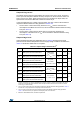
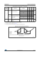
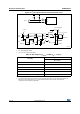
Figure 39. Recommended NRST pin protection
1. The reset network protects the device against parasitic resets.
2. The user must ensure that the level on the NRST pin can go below the V
IL(NRST)
max level specified in
Table 49. Otherwise the reset is not taken into account by the device.
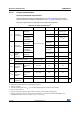
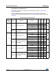
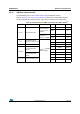
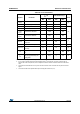
Table 49. NRST pin characteristics
Symbol Parameter Conditions Min Typ Max Unit
V
IL(NRST)
(1)
NRST input low level voltage
TTL ports
2.7 V ≤
V
DD
≤ 3.6 V
--0.8
V
V
IH(NRST)
(1)
NRST input high level voltage 2 - -
V
IL(NRST)
(1)
NRST input low level voltage
CMOS ports
1.8 V ≤
V
DD
≤ 3.6 V
- - 0.3V
DD
V
V
IH(NRST)
(1)
NRST input high level voltage 0.7V
DD
--
V
hys(NRST)
NRST Schmitt trigger voltage
hysteresis
-200-mV
R
PU
Weak pull-up equivalent resistor
(2)
V
IN
= V
SS
30 40 50 kΩ
V
F(NRST)
(1)
NRST Input filtered pulse - - 100 ns
V
NF(NRST)
(1)
NRST Input not filtered pulse V
DD
> 2.7 V 300 - - ns
T
NRST_OUT
Generated reset pulse duration Internal Reset source 20 - - µs
1. Guaranteed by design, not tested in production.
2. The pull-up is designed with a true resistance in series with a switchable PMOS. This PMOS contribution
to the series
resistance must be minimum
(~10% order).
ai14132c
STM32Fxxx
R
PU
NRST
(2)
V
DD
Filter
Internal Reset
0.1 μF
External
reset circuit
(1)