
Datasheet


DocID15818 Rev 11 123/178
STM32F20xxx Electrical characteristics
177
being performed on another analog input. It is recommended to add a Schottky diode (pin to
ground) to analog pins which may potentially inject negative currents.
Any positive injection current within the limits specified for I
INJ(PIN)
and ΣI
INJ(PIN)
in
Section 6.3.16 does not affect the ADC accuracy.
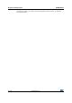
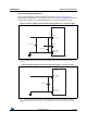
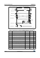
Figure 51. ADC accuracy characteristics
1. Example of an actual transfer curve.
2. Ideal transfer curve.
3. End point correlation line.
4. E
T
= Total Unadjusted Error: maximum deviation between the actual and the ideal transfer curves.
EO = Offset Error: deviation between the first actual transition and the first ideal one.
EG = Gain Error: deviation between the last ideal transition and the last actual one.
ED = Differential Linearity Error: maximum deviation between actual steps and the ideal one.
EL = Integral Linearity Error: maximum deviation between any actual transition and the end point
correlation line.
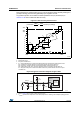
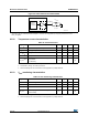
Figure 52. Typical connection diagram using the ADC
1. Refer to Table 66 for the values of R
AIN
, R
ADC
and C
ADC
.
2. C
parasitic
represents the capacitance of the PCB (dependent on soldering and PCB layout quality) plus the
ai14395c
E
O
E
G
1L SB
IDEAL
4095
4094
4093
5
4
3
2
1
0
7
6
1 2 3 456 7
4093 4094 4095 4096
(1)
(2)
E
T
E
D
E
L
(3)
V
DDA
V
SSA
V
REF+
4096
(or depending on package)]
V
DDA
4096
[1LSB
IDEAL
=
ai17534
STM32F
V
DD
AINx
I
L
±1 µA
0.6 V
V
T
R
AIN
(1)
C
parasitic
V
AIN
0.6 V
V
T
R
ADC
(1)
C
ADC
(1)
12-bit
converter
Sample and hold ADC
converter