
Datasheet


Electrical characteristics STM32F20xxx
70/178 DocID15818 Rev 11
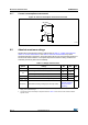
V
BAT
Backup operating voltage 1.65 3.6
V
V
IN
I/O input voltage
FT and TTa I/O TBD TBD
BOOT0 TBD TBD
V
CAP1
Internal core voltage to be supplied
externally in REGOFF mode
1.1 1.3 V
V
CAP2
P
D
Power dissipation at T
A
= 85 °C for
suffix 6 or T
A
= 105 °C for suffix 7
(5)
LQFP64 - 444
mW
WLCSP64+2 - 392
LQFP100 - 434
LQFP144 - 500
LQFP176 - 526
UFBGA176 - 513
T
A
Ambient temperature for 6 suffix
version
Maximum power dissipation –40 85
°C
Low power dissipation
(6)
–40 105
Ambient temperature for 7 suffix
version
Maximum power dissipation –40 105
°C
Low power dissipation
(6)
–40 125
T
J Junction temperature range
6 suffix version –40 105
°C
7 suffix version –40 125
1. TBD stands for “to be defined”.
2. On devices in WLCSP64+2 package, if IRROFF is set to V
DD
, the supply voltage can drop to 1.7 V when the device
operates in the 0 to 70 °C temperature range using an external power supply supervisor (see Section 3.16).
3. When the ADC is used, refer to Table 66: ADC characteristics.
4. It is recommended to power V
DD
and V
DDA
from the same source. A maximum difference of 300 mV between V
DD
and
V
DDA
can be tolerated during power-up and power-down operation.
5. If T
A
is lower, higher P
D
values are allowed as long as T
J
does not exceed T
Jmax
.
6. In low power dissipation state, T
A
can be extended to this range as long as T
J
does not exceed T
Jmax
.
Table 14. General operating conditions
(1)
(continued)
Symbol Parameter Conditions Min Max Unit