
Datasheet
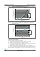
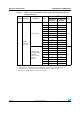
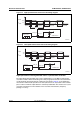
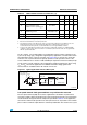
Table Of Contents
- Table 1. Device summary
- 1 Introduction
- 2 Description
- 2.1 Device overview
- 2.2 Full compatibility throughout the family
- 2.3 Overview
- Figure 1. STM32F105xx and STM32F107xx connectivity line block diagram
- 2.3.1 ARM® Cortex™-M3 core with embedded Flash and SRAM
- 2.3.2 Embedded Flash memory
- 2.3.3 CRC (cyclic redundancy check) calculation unit
- 2.3.4 Embedded SRAM
- 2.3.5 Nested vectored interrupt controller (NVIC)
- 2.3.6 External interrupt/event controller (EXTI)
- 2.3.7 Clocks and startup
- 2.3.8 Boot modes
- 2.3.9 Power supply schemes
- 2.3.10 Power supply supervisor
- 2.3.11 Voltage regulator
- 2.3.12 Low-power modes
- 2.3.13 DMA
- 2.3.14 RTC (real-time clock) and backup registers
- 2.3.15 Timers and watchdogs
- 2.3.16 I²C bus
- 2.3.17 Universal synchronous/asynchronous receiver transmitters (USARTs)
- 2.3.18 Serial peripheral interface (SPI)
- 2.3.19 Inter-integrated sound (I2S)
- 2.3.20 Ethernet MAC interface with dedicated DMA and IEEE 1588 support
- 2.3.21 Controller area network (CAN)
- 2.3.22 Universal serial bus on-the-go full-speed (USB OTG FS)
- 2.3.23 GPIOs (general-purpose inputs/outputs)
- 2.3.24 Remap capability
- 2.3.25 ADCs (analog-to-digital converters)
- 2.3.26 DAC (digital-to-analog converter)
- 2.3.27 Temperature sensor
- 2.3.28 Serial wire JTAG debug port (SWJ-DP)
- 2.3.29 Embedded Trace Macrocell™
- 3 Pinouts and pin description
- 4 Memory mapping
- 5 Electrical characteristics
- 5.1 Parameter conditions
- 5.2 Absolute maximum ratings
- 5.3 Operating conditions
- 5.3.1 General operating conditions
- 5.3.2 Operating conditions at power-up / power-down
- 5.3.3 Embedded reset and power control block characteristics
- 5.3.4 Embedded reference voltage
- 5.3.5 Supply current characteristics
- Table 13. Maximum current consumption in Run mode, code with data processing running from Flash
- Table 14. Maximum current consumption in Run mode, code with data processing running from RAM
- Table 15. Maximum current consumption in Sleep mode, code running from Flash or RAM
- Table 16. Typical and maximum current consumptions in Stop and Standby modes
- Figure 10. Typical current consumption on VBAT with RTC on vs. temperature at different VBAT values
- Figure 11. Typical current consumption in Stop mode with regulator in Run mode versus temperature at different VDD values
- Figure 12. Typical current consumption in Stop mode with regulator in Low-power mode versus temperature at different VDD values
- Figure 13. Typical current consumption in Standby mode versus temperature at different VDD values
- Table 17. Typical current consumption in Run mode, code with data processing running from Flash
- Table 18. Typical current consumption in Sleep mode, code running from Flash or RAM
- Table 19. Peripheral current consumption
- 5.3.6 External clock source characteristics
- Table 20. High-speed external user clock characteristics
- Table 21. Low-speed external user clock characteristics
- Figure 14. High-speed external clock source AC timing diagram
- Figure 15. Low-speed external clock source AC timing diagram
- Table 22. HSE 3-25 MHz oscillator characteristics
- Figure 16. Typical application with an 8 MHz crystal
- Table 23. LSE oscillator characteristics (fLSE = 32.768 kHz)
- Figure 17. Typical application with a 32.768 kHz crystal
- 5.3.7 Internal clock source characteristics
- 5.3.8 PLL, PLL2 and PLL3 characteristics
- 5.3.9 Memory characteristics
- 5.3.10 EMC characteristics
- 5.3.11 Absolute maximum ratings (electrical sensitivity)
- 5.3.12 I/O current injection characteristics
- 5.3.13 I/O port characteristics
- Table 36. I/O static characteristics
- Figure 18. Standard I/O input characteristics - CMOS port
- Figure 19. Standard I/O input characteristics - TTL port
- Figure 20. 5 V tolerant I/O input characteristics - CMOS port
- Figure 21. 5 V tolerant I/O input characteristics - TTL port
- Table 37. Output voltage characteristics
- Table 38. I/O AC characteristics
- Figure 22. I/O AC characteristics definition
- 5.3.14 NRST pin characteristics
- 5.3.15 TIM timer characteristics
- 5.3.16 Communications interfaces
- Table 41. I2C characteristics
- Figure 24. I2C bus AC waveforms and measurement circuit
- Table 42. SCL frequency (fPCLK1= 36 MHz.,VDD = 3.3 V)
- Table 43. SPI characteristics
- Figure 25. SPI timing diagram - slave mode and CPHA = 0
- Figure 26. SPI timing diagram - slave mode and CPHA = 1(1)
- Figure 27. SPI timing diagram - master mode(1)
- Table 44. I2S characteristics
- Figure 28. I2S slave timing diagram (Philips protocol)(1)
- Figure 29. I2S master timing diagram (Philips protocol)(1)
- Table 45. USB OTG FS startup time
- Table 46. USB OTG FS DC electrical characteristics
- Figure 30. USB OTG FS timings: definition of data signal rise and fall time
- Table 47. USB OTG FS electrical characteristics
- Table 48. Ethernet DC electrical characteristics
- Figure 31. Ethernet SMI timing diagram
- Table 49. Dynamic characteristics: Ethernet MAC signals for SMI
- Figure 32. Ethernet RMII timing diagram
- Table 50. Dynamic characteristics: Ethernet MAC signals for RMII
- Figure 33. Ethernet MII timing diagram
- Table 51. Dynamic characteristics: Ethernet MAC signals for MII
- 5.3.17 12-bit ADC characteristics
- Table 52. ADC characteristics
- Table 53. RAIN max for fADC = 14 MHz
- Table 54. ADC accuracy - limited test conditions
- Table 55. ADC accuracy
- Figure 34. ADC accuracy characteristics
- Figure 35. Typical connection diagram using the ADC
- Figure 36. Power supply and reference decoupling (VREF+ not connected to VDDA)
- Figure 37. Power supply and reference decoupling (VREF+ connected to VDDA)
- 5.3.18 DAC electrical specifications
- 5.3.19 Temperature sensor characteristics
- 6 Package characteristics
- 6.1 Package mechanical data
- Figure 39. LFBGA100 - 10 x 10 mm low profile fine pitch ball grid array package outline
- Table 58. LFBGA100 - 10 x 10 mm low profile fine pitch ball grid array package mechanical data
- Figure 40. Recommended PCB design rules (0.80/0.75 mm pitch BGA)
- Figure 41. LQFP100, 100-pin low-profile quad flat package outline
- Figure 42. Recommended footprint(1)
- Table 59. LQPF100 – 100-pin low-profile quad flat package mechanical data
- Figure 43. LQFP64 – 64 pin low-profile quad flat package outline
- Figure 44. Recommended footprint(1)
- Table 60. LQFP64 – 64 pin low-profile quad flat package mechanical data
- 6.2 Thermal characteristics
- 6.1 Package mechanical data
- 7 Part numbering
- Appendix A Application block diagrams
- Revision history
STM32F105xx, STM32F107xx Electrical characteristics
Doc ID 15274 Rev 6 47/104
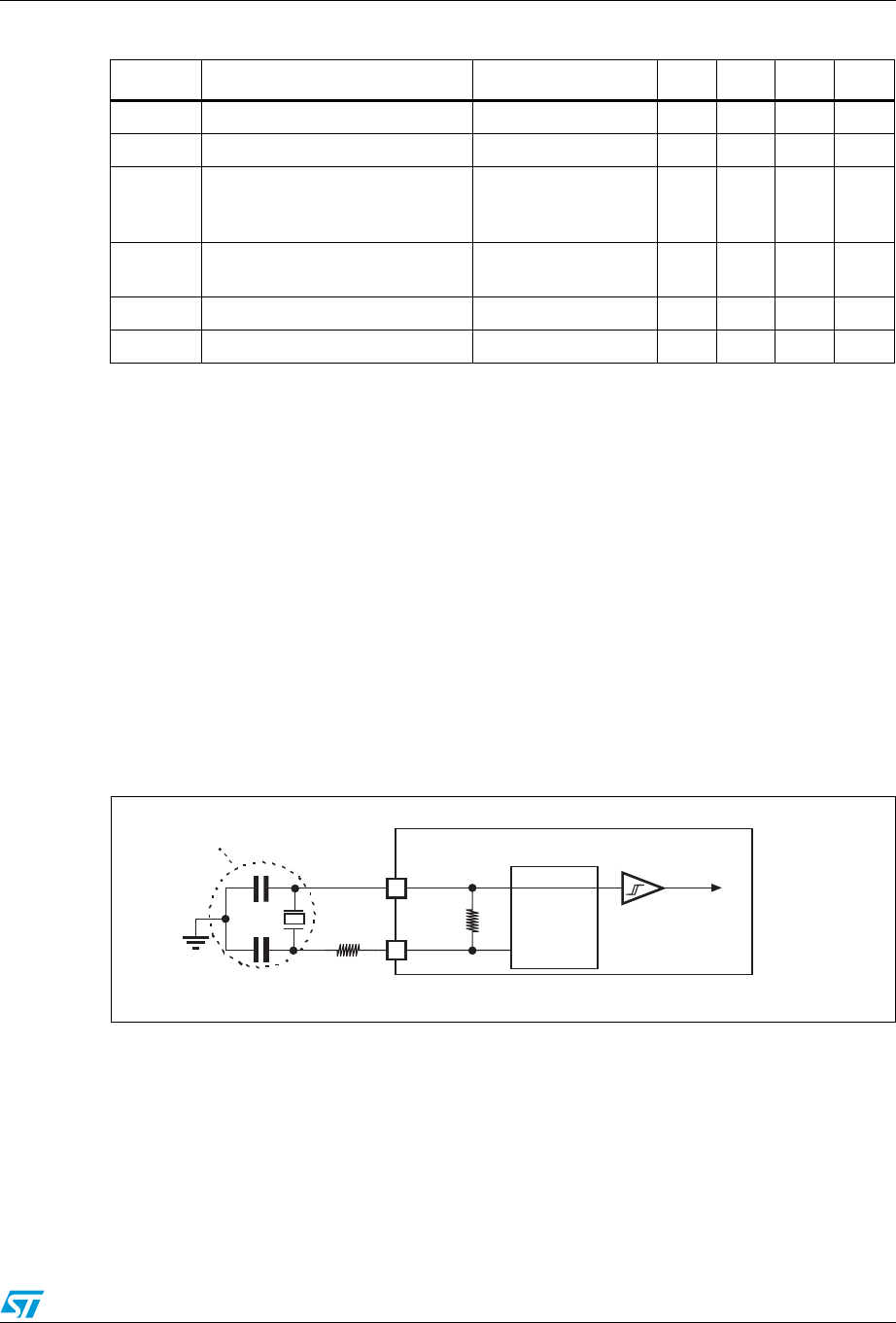
For C
L1
and C
L2
, it is recommended to use high-quality external ceramic capacitors in the
5 pF to 25 pF range (typ.), designed for high-frequency applications, and selected to match
the requirements of the crystal or resonator (see Figure 16). C
L1
and C
L2
are usually the
same size. The crystal manufacturer typically specifies a load capacitance which is the
series combination of C
L1
and C
L2
. PCB and MCU pin capacitance must be included (10 pF
can be used as a rough estimate of the combined pin and board capacitance) when sizing
C
L1
and C
L2
. Refer to the application note AN2867 “Oscillator design guide for ST
microcontrollers” available from the ST website www.st.com.
Figure 16. Typical application with an 8 MHz crystal
1. R
EXT
value depends on the crystal characteristics.
Low-speed external clock generated from a crystal/ceramic resonator
The low-speed external (LSE) clock can be supplied with a 32.768 kHz crystal/ceramic
resonator oscillator. All the information given in this paragraph are based on characterization
results obtained with typical external components specified in Tabl e 23. In the application,
the resonator and the load capacitors have to be placed as close as possible to the oscillator
pins in order to minimize output distortion and startup stabilization time. Refer to the crystal
Table 22. HSE 3-25 MHz oscillator characteristics
(1)
(2)
1. Resonator characteristics given by the crystal/ceramic resonator manufacturer.
2. Based on characterization, not tested in production.
Symbol Parameter Conditions Min Typ Max Unit
f
OSC_IN
Oscillator frequency 3 25 MHz
R
F
Feedback resistor 200 kΩ
C
Recommended load capacitance
versus equivalent serial
resistance of the crystal (R
S
)
(3)
3. The relatively low value of the RF resistor offers a good protection against issues resulting from use in a
humid environment, due to the induced leakage and the bias condition change. However, it is
recommended to take this point into account if the MCU is used in tough humidity conditions.
R
S
= 30 Ω 30 pF
i
2
HSE driving current
V
DD
= 3.3 V, V
IN
=V
SS
with 30 pF load
1mA
g
m
Oscillator transconductance Startup 25 mA/V
t
SU(HSE
(4)
4. t
SU(HSE)
is the startup time measured from the moment it is enabled (by software) to a stabilized 8 MHz
oscillation is reached. This value is measured for a standard crystal resonator and it can vary significantly
with the crystal manufacturer
Startup time V
DD
is stabilized 2 ms
ai14128b
OSC_OU T
OSC_IN
f
HSE
C
L1
R
F
STM32F10xxx
8 MHz
resonator
Resonator with
integrated capacitors
Bias
controlled
gain
R
EXT
(1)
C
L2