
Datasheet
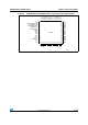
Table Of Contents
- Table 1. Device summary
- 1 Introduction
- 2 Description
- 2.1 Device overview
- 2.2 Full compatibility throughout the family
- 2.3 Overview
- Figure 1. STM32F105xx and STM32F107xx connectivity line block diagram
- 2.3.1 ARM® Cortex™-M3 core with embedded Flash and SRAM
- 2.3.2 Embedded Flash memory
- 2.3.3 CRC (cyclic redundancy check) calculation unit
- 2.3.4 Embedded SRAM
- 2.3.5 Nested vectored interrupt controller (NVIC)
- 2.3.6 External interrupt/event controller (EXTI)
- 2.3.7 Clocks and startup
- 2.3.8 Boot modes
- 2.3.9 Power supply schemes
- 2.3.10 Power supply supervisor
- 2.3.11 Voltage regulator
- 2.3.12 Low-power modes
- 2.3.13 DMA
- 2.3.14 RTC (real-time clock) and backup registers
- 2.3.15 Timers and watchdogs
- 2.3.16 I²C bus
- 2.3.17 Universal synchronous/asynchronous receiver transmitters (USARTs)
- 2.3.18 Serial peripheral interface (SPI)
- 2.3.19 Inter-integrated sound (I2S)
- 2.3.20 Ethernet MAC interface with dedicated DMA and IEEE 1588 support
- 2.3.21 Controller area network (CAN)
- 2.3.22 Universal serial bus on-the-go full-speed (USB OTG FS)
- 2.3.23 GPIOs (general-purpose inputs/outputs)
- 2.3.24 Remap capability
- 2.3.25 ADCs (analog-to-digital converters)
- 2.3.26 DAC (digital-to-analog converter)
- 2.3.27 Temperature sensor
- 2.3.28 Serial wire JTAG debug port (SWJ-DP)
- 2.3.29 Embedded Trace Macrocell™
- 3 Pinouts and pin description
- 4 Memory mapping
- 5 Electrical characteristics
- 5.1 Parameter conditions
- 5.2 Absolute maximum ratings
- 5.3 Operating conditions
- 5.3.1 General operating conditions
- 5.3.2 Operating conditions at power-up / power-down
- 5.3.3 Embedded reset and power control block characteristics
- 5.3.4 Embedded reference voltage
- 5.3.5 Supply current characteristics
- Table 13. Maximum current consumption in Run mode, code with data processing running from Flash
- Table 14. Maximum current consumption in Run mode, code with data processing running from RAM
- Table 15. Maximum current consumption in Sleep mode, code running from Flash or RAM
- Table 16. Typical and maximum current consumptions in Stop and Standby modes
- Figure 10. Typical current consumption on VBAT with RTC on vs. temperature at different VBAT values
- Figure 11. Typical current consumption in Stop mode with regulator in Run mode versus temperature at different VDD values
- Figure 12. Typical current consumption in Stop mode with regulator in Low-power mode versus temperature at different VDD values
- Figure 13. Typical current consumption in Standby mode versus temperature at different VDD values
- Table 17. Typical current consumption in Run mode, code with data processing running from Flash
- Table 18. Typical current consumption in Sleep mode, code running from Flash or RAM
- Table 19. Peripheral current consumption
- 5.3.6 External clock source characteristics
- Table 20. High-speed external user clock characteristics
- Table 21. Low-speed external user clock characteristics
- Figure 14. High-speed external clock source AC timing diagram
- Figure 15. Low-speed external clock source AC timing diagram
- Table 22. HSE 3-25 MHz oscillator characteristics
- Figure 16. Typical application with an 8 MHz crystal
- Table 23. LSE oscillator characteristics (fLSE = 32.768 kHz)
- Figure 17. Typical application with a 32.768 kHz crystal
- 5.3.7 Internal clock source characteristics
- 5.3.8 PLL, PLL2 and PLL3 characteristics
- 5.3.9 Memory characteristics
- 5.3.10 EMC characteristics
- 5.3.11 Absolute maximum ratings (electrical sensitivity)
- 5.3.12 I/O current injection characteristics
- 5.3.13 I/O port characteristics
- Table 36. I/O static characteristics
- Figure 18. Standard I/O input characteristics - CMOS port
- Figure 19. Standard I/O input characteristics - TTL port
- Figure 20. 5 V tolerant I/O input characteristics - CMOS port
- Figure 21. 5 V tolerant I/O input characteristics - TTL port
- Table 37. Output voltage characteristics
- Table 38. I/O AC characteristics
- Figure 22. I/O AC characteristics definition
- 5.3.14 NRST pin characteristics
- 5.3.15 TIM timer characteristics
- 5.3.16 Communications interfaces
- Table 41. I2C characteristics
- Figure 24. I2C bus AC waveforms and measurement circuit
- Table 42. SCL frequency (fPCLK1= 36 MHz.,VDD = 3.3 V)
- Table 43. SPI characteristics
- Figure 25. SPI timing diagram - slave mode and CPHA = 0
- Figure 26. SPI timing diagram - slave mode and CPHA = 1(1)
- Figure 27. SPI timing diagram - master mode(1)
- Table 44. I2S characteristics
- Figure 28. I2S slave timing diagram (Philips protocol)(1)
- Figure 29. I2S master timing diagram (Philips protocol)(1)
- Table 45. USB OTG FS startup time
- Table 46. USB OTG FS DC electrical characteristics
- Figure 30. USB OTG FS timings: definition of data signal rise and fall time
- Table 47. USB OTG FS electrical characteristics
- Table 48. Ethernet DC electrical characteristics
- Figure 31. Ethernet SMI timing diagram
- Table 49. Dynamic characteristics: Ethernet MAC signals for SMI
- Figure 32. Ethernet RMII timing diagram
- Table 50. Dynamic characteristics: Ethernet MAC signals for RMII
- Figure 33. Ethernet MII timing diagram
- Table 51. Dynamic characteristics: Ethernet MAC signals for MII
- 5.3.17 12-bit ADC characteristics
- Table 52. ADC characteristics
- Table 53. RAIN max for fADC = 14 MHz
- Table 54. ADC accuracy - limited test conditions
- Table 55. ADC accuracy
- Figure 34. ADC accuracy characteristics
- Figure 35. Typical connection diagram using the ADC
- Figure 36. Power supply and reference decoupling (VREF+ not connected to VDDA)
- Figure 37. Power supply and reference decoupling (VREF+ connected to VDDA)
- 5.3.18 DAC electrical specifications
- 5.3.19 Temperature sensor characteristics
- 6 Package characteristics
- 6.1 Package mechanical data
- Figure 39. LFBGA100 - 10 x 10 mm low profile fine pitch ball grid array package outline
- Table 58. LFBGA100 - 10 x 10 mm low profile fine pitch ball grid array package mechanical data
- Figure 40. Recommended PCB design rules (0.80/0.75 mm pitch BGA)
- Figure 41. LQFP100, 100-pin low-profile quad flat package outline
- Figure 42. Recommended footprint(1)
- Table 59. LQPF100 – 100-pin low-profile quad flat package mechanical data
- Figure 43. LQFP64 – 64 pin low-profile quad flat package outline
- Figure 44. Recommended footprint(1)
- Table 60. LQFP64 – 64 pin low-profile quad flat package mechanical data
- 6.2 Thermal characteristics
- 6.1 Package mechanical data
- 7 Part numbering
- Appendix A Application block diagrams
- Revision history
STM32F105xx, STM32F107xx Pinouts and pin description
Doc ID 15274 Rev 6 25/104
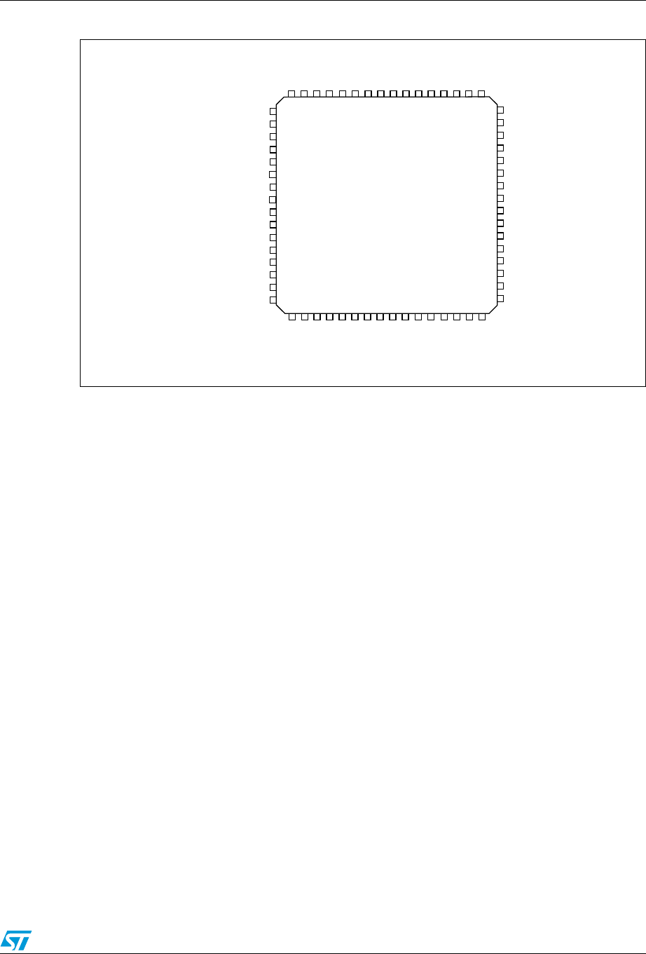
Figure 4. STM32F105xxx and STM32F107xxx connectivity line LQFP64 pinout
64 63 62 61 60 59 58 57 56 55 54 53 52 51 50 49
48
47
46
45
44
43
42
41
40
39
38
37
36
35
34
33
17 18 19 20 21 22 23 24 29 30 31 3225 26 27 28
1
2
3
4
5
6
7
8
9
10
11
12
13
14
15
16
V
BAT
PC13-TAMPER-RTC
PC14-OSC32_IN
PC15-OSC32_OUT
PD0 OSC_IN
PD1 OSC_OUT
NRST
PC0
PC1
PC2
PC3
V
SSA
V
DDA
PA0 - WKUP
PA1
PA2
V
DD_3
V
SS_3
PB9
PB8
BOOT0
PB7
PB6
PB5
PB4
PB3
PD2
PC12
PC11
PC10
PA 1 5
PA 1 4
V
DD_2
V
SS_2
PA 1 3
PA 1 2
PA 1 1
PA 1 0
PA 9
PA 8
PC9
PC8
PC7
PC6
PB15
PB14
PB13
PB12
PA3
V
SS_4
V
DD_4
PA4
PA5
PA6
PA7
PC4
PC5
PB0
PB1
PB2
PB10
PB11
V
SS_1
V
DD_1
LQFP64
ai14392