
Datasheet
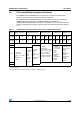
Table Of Contents
- Table 1. Device summary
- 1 Introduction
- 2 Description
- 2.1 Device overview
- 2.2 Full compatibility throughout the family
- 2.3 Overview
- Figure 1. STM32F105xx and STM32F107xx connectivity line block diagram
- 2.3.1 ARM® Cortex™-M3 core with embedded Flash and SRAM
- 2.3.2 Embedded Flash memory
- 2.3.3 CRC (cyclic redundancy check) calculation unit
- 2.3.4 Embedded SRAM
- 2.3.5 Nested vectored interrupt controller (NVIC)
- 2.3.6 External interrupt/event controller (EXTI)
- 2.3.7 Clocks and startup
- 2.3.8 Boot modes
- 2.3.9 Power supply schemes
- 2.3.10 Power supply supervisor
- 2.3.11 Voltage regulator
- 2.3.12 Low-power modes
- 2.3.13 DMA
- 2.3.14 RTC (real-time clock) and backup registers
- 2.3.15 Timers and watchdogs
- 2.3.16 I²C bus
- 2.3.17 Universal synchronous/asynchronous receiver transmitters (USARTs)
- 2.3.18 Serial peripheral interface (SPI)
- 2.3.19 Inter-integrated sound (I2S)
- 2.3.20 Ethernet MAC interface with dedicated DMA and IEEE 1588 support
- 2.3.21 Controller area network (CAN)
- 2.3.22 Universal serial bus on-the-go full-speed (USB OTG FS)
- 2.3.23 GPIOs (general-purpose inputs/outputs)
- 2.3.24 Remap capability
- 2.3.25 ADCs (analog-to-digital converters)
- 2.3.26 DAC (digital-to-analog converter)
- 2.3.27 Temperature sensor
- 2.3.28 Serial wire JTAG debug port (SWJ-DP)
- 2.3.29 Embedded Trace Macrocell™
- 3 Pinouts and pin description
- 4 Memory mapping
- 5 Electrical characteristics
- 5.1 Parameter conditions
- 5.2 Absolute maximum ratings
- 5.3 Operating conditions
- 5.3.1 General operating conditions
- 5.3.2 Operating conditions at power-up / power-down
- 5.3.3 Embedded reset and power control block characteristics
- 5.3.4 Embedded reference voltage
- 5.3.5 Supply current characteristics
- Table 13. Maximum current consumption in Run mode, code with data processing running from Flash
- Table 14. Maximum current consumption in Run mode, code with data processing running from RAM
- Table 15. Maximum current consumption in Sleep mode, code running from Flash or RAM
- Table 16. Typical and maximum current consumptions in Stop and Standby modes
- Figure 10. Typical current consumption on VBAT with RTC on vs. temperature at different VBAT values
- Figure 11. Typical current consumption in Stop mode with regulator in Run mode versus temperature at different VDD values
- Figure 12. Typical current consumption in Stop mode with regulator in Low-power mode versus temperature at different VDD values
- Figure 13. Typical current consumption in Standby mode versus temperature at different VDD values
- Table 17. Typical current consumption in Run mode, code with data processing running from Flash
- Table 18. Typical current consumption in Sleep mode, code running from Flash or RAM
- Table 19. Peripheral current consumption
- 5.3.6 External clock source characteristics
- Table 20. High-speed external user clock characteristics
- Table 21. Low-speed external user clock characteristics
- Figure 14. High-speed external clock source AC timing diagram
- Figure 15. Low-speed external clock source AC timing diagram
- Table 22. HSE 3-25 MHz oscillator characteristics
- Figure 16. Typical application with an 8 MHz crystal
- Table 23. LSE oscillator characteristics (fLSE = 32.768 kHz)
- Figure 17. Typical application with a 32.768 kHz crystal
- 5.3.7 Internal clock source characteristics
- 5.3.8 PLL, PLL2 and PLL3 characteristics
- 5.3.9 Memory characteristics
- 5.3.10 EMC characteristics
- 5.3.11 Absolute maximum ratings (electrical sensitivity)
- 5.3.12 I/O current injection characteristics
- 5.3.13 I/O port characteristics
- Table 36. I/O static characteristics
- Figure 18. Standard I/O input characteristics - CMOS port
- Figure 19. Standard I/O input characteristics - TTL port
- Figure 20. 5 V tolerant I/O input characteristics - CMOS port
- Figure 21. 5 V tolerant I/O input characteristics - TTL port
- Table 37. Output voltage characteristics
- Table 38. I/O AC characteristics
- Figure 22. I/O AC characteristics definition
- 5.3.14 NRST pin characteristics
- 5.3.15 TIM timer characteristics
- 5.3.16 Communications interfaces
- Table 41. I2C characteristics
- Figure 24. I2C bus AC waveforms and measurement circuit
- Table 42. SCL frequency (fPCLK1= 36 MHz.,VDD = 3.3 V)
- Table 43. SPI characteristics
- Figure 25. SPI timing diagram - slave mode and CPHA = 0
- Figure 26. SPI timing diagram - slave mode and CPHA = 1(1)
- Figure 27. SPI timing diagram - master mode(1)
- Table 44. I2S characteristics
- Figure 28. I2S slave timing diagram (Philips protocol)(1)
- Figure 29. I2S master timing diagram (Philips protocol)(1)
- Table 45. USB OTG FS startup time
- Table 46. USB OTG FS DC electrical characteristics
- Figure 30. USB OTG FS timings: definition of data signal rise and fall time
- Table 47. USB OTG FS electrical characteristics
- Table 48. Ethernet DC electrical characteristics
- Figure 31. Ethernet SMI timing diagram
- Table 49. Dynamic characteristics: Ethernet MAC signals for SMI
- Figure 32. Ethernet RMII timing diagram
- Table 50. Dynamic characteristics: Ethernet MAC signals for RMII
- Figure 33. Ethernet MII timing diagram
- Table 51. Dynamic characteristics: Ethernet MAC signals for MII
- 5.3.17 12-bit ADC characteristics
- Table 52. ADC characteristics
- Table 53. RAIN max for fADC = 14 MHz
- Table 54. ADC accuracy - limited test conditions
- Table 55. ADC accuracy
- Figure 34. ADC accuracy characteristics
- Figure 35. Typical connection diagram using the ADC
- Figure 36. Power supply and reference decoupling (VREF+ not connected to VDDA)
- Figure 37. Power supply and reference decoupling (VREF+ connected to VDDA)
- 5.3.18 DAC electrical specifications
- 5.3.19 Temperature sensor characteristics
- 6 Package characteristics
- 6.1 Package mechanical data
- Figure 39. LFBGA100 - 10 x 10 mm low profile fine pitch ball grid array package outline
- Table 58. LFBGA100 - 10 x 10 mm low profile fine pitch ball grid array package mechanical data
- Figure 40. Recommended PCB design rules (0.80/0.75 mm pitch BGA)
- Figure 41. LQFP100, 100-pin low-profile quad flat package outline
- Figure 42. Recommended footprint(1)
- Table 59. LQPF100 – 100-pin low-profile quad flat package mechanical data
- Figure 43. LQFP64 – 64 pin low-profile quad flat package outline
- Figure 44. Recommended footprint(1)
- Table 60. LQFP64 – 64 pin low-profile quad flat package mechanical data
- 6.2 Thermal characteristics
- 6.1 Package mechanical data
- 7 Part numbering
- Appendix A Application block diagrams
- Revision history

STM32F105xx, STM32F107xx Description
Doc ID 15274 Rev 6 15/104
2.3.9 Power supply schemes
● V
DD
= 2.0 to 3.6 V: external power supply for I/Os and the internal regulator.
Provided externally through V
DD
pins.
● V
SSA
, V
DDA
= 2.0 to 3.6 V: external analog power supplies for ADC, Reset blocks, RCs
and PLL (minimum voltage to be applied to V
DDA
is 2.4 V when the ADC is used). V
DDA
and V
SSA
must be connected to V
DD
and V
SS
, respectively.
● V
BAT
= 1.8 to 3.6 V: power supply for RTC, external clock 32 kHz oscillator and backup
registers (through power switch) when V
DD
is not present.
2.3.10 Power supply supervisor
The device has an integrated power-on reset (POR)/power-down reset (PDR) circuitry. It is
always active, and ensures proper operation starting from/down to 2 V. The device remains
in reset mode when V
DD
is below a specified threshold, V
POR/PDR
, without the need for an
external reset circuit.
The device features an embedded programmable voltage detector (PVD) that monitors the
V
DD
/V
DDA
power supply and compares it to the V
PVD
threshold. An interrupt can be
generated when V
DD
/V
DDA
drops below the V
PVD
threshold and/or when V
DD
/V
DDA
is higher
than the V
PVD
threshold. The interrupt service routine can then generate a warning
message and/or put the MCU into a safe state. The PVD is enabled by software.
2.3.11 Voltage regulator
The regulator has three operation modes: main (MR), low power (LPR) and power down.
● MR is used in the nominal regulation mode (Run)
● LPR is used in the Stop modes.
● Power down is used in Standby mode: the regulator output is in high impedance: the
kernel circuitry is powered down, inducing zero consumption (but the contents of the
registers and SRAM are lost)
This regulator is always enabled after reset. It is disabled in Standby mode.
2.3.12 Low-power modes
The STM32F105xx and STM32F107xx connectivity line supports three low-power modes to
achieve the best compromise between low power consumption, short startup time and
available wakeup sources:
● Sleep mode
In Sleep mode, only the CPU is stopped. All peripherals continue to operate and can
wake up the CPU when an interrupt/event occurs.
● Stop mode
Stop mode achieves the lowest power consumption while retaining the content of
SRAM and registers. All clocks in the 1.8 V domain are stopped, the PLL, the HSI RC
and the HSE crystal oscillators are disabled. The voltage regulator can also be put
either in normal or in low-power mode.
The device can be woken up from Stop mode by any of the EXTI line. The EXTI line
source can be one of the 16 external lines, the PVD output, the RTC alarm or the USB
OTG FS wakeup.