
Datasheet
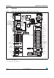
Table Of Contents
- Table 1. Device summary
- 1 Introduction
- 2 Description
- 2.1 Device overview
- 2.2 Full compatibility throughout the family
- 2.3 Overview
- Figure 1. STM32F105xx and STM32F107xx connectivity line block diagram
- 2.3.1 ARM® Cortex™-M3 core with embedded Flash and SRAM
- 2.3.2 Embedded Flash memory
- 2.3.3 CRC (cyclic redundancy check) calculation unit
- 2.3.4 Embedded SRAM
- 2.3.5 Nested vectored interrupt controller (NVIC)
- 2.3.6 External interrupt/event controller (EXTI)
- 2.3.7 Clocks and startup
- 2.3.8 Boot modes
- 2.3.9 Power supply schemes
- 2.3.10 Power supply supervisor
- 2.3.11 Voltage regulator
- 2.3.12 Low-power modes
- 2.3.13 DMA
- 2.3.14 RTC (real-time clock) and backup registers
- 2.3.15 Timers and watchdogs
- 2.3.16 I²C bus
- 2.3.17 Universal synchronous/asynchronous receiver transmitters (USARTs)
- 2.3.18 Serial peripheral interface (SPI)
- 2.3.19 Inter-integrated sound (I2S)
- 2.3.20 Ethernet MAC interface with dedicated DMA and IEEE 1588 support
- 2.3.21 Controller area network (CAN)
- 2.3.22 Universal serial bus on-the-go full-speed (USB OTG FS)
- 2.3.23 GPIOs (general-purpose inputs/outputs)
- 2.3.24 Remap capability
- 2.3.25 ADCs (analog-to-digital converters)
- 2.3.26 DAC (digital-to-analog converter)
- 2.3.27 Temperature sensor
- 2.3.28 Serial wire JTAG debug port (SWJ-DP)
- 2.3.29 Embedded Trace Macrocell™
- 3 Pinouts and pin description
- 4 Memory mapping
- 5 Electrical characteristics
- 5.1 Parameter conditions
- 5.2 Absolute maximum ratings
- 5.3 Operating conditions
- 5.3.1 General operating conditions
- 5.3.2 Operating conditions at power-up / power-down
- 5.3.3 Embedded reset and power control block characteristics
- 5.3.4 Embedded reference voltage
- 5.3.5 Supply current characteristics
- Table 13. Maximum current consumption in Run mode, code with data processing running from Flash
- Table 14. Maximum current consumption in Run mode, code with data processing running from RAM
- Table 15. Maximum current consumption in Sleep mode, code running from Flash or RAM
- Table 16. Typical and maximum current consumptions in Stop and Standby modes
- Figure 10. Typical current consumption on VBAT with RTC on vs. temperature at different VBAT values
- Figure 11. Typical current consumption in Stop mode with regulator in Run mode versus temperature at different VDD values
- Figure 12. Typical current consumption in Stop mode with regulator in Low-power mode versus temperature at different VDD values
- Figure 13. Typical current consumption in Standby mode versus temperature at different VDD values
- Table 17. Typical current consumption in Run mode, code with data processing running from Flash
- Table 18. Typical current consumption in Sleep mode, code running from Flash or RAM
- Table 19. Peripheral current consumption
- 5.3.6 External clock source characteristics
- Table 20. High-speed external user clock characteristics
- Table 21. Low-speed external user clock characteristics
- Figure 14. High-speed external clock source AC timing diagram
- Figure 15. Low-speed external clock source AC timing diagram
- Table 22. HSE 3-25 MHz oscillator characteristics
- Figure 16. Typical application with an 8 MHz crystal
- Table 23. LSE oscillator characteristics (fLSE = 32.768 kHz)
- Figure 17. Typical application with a 32.768 kHz crystal
- 5.3.7 Internal clock source characteristics
- 5.3.8 PLL, PLL2 and PLL3 characteristics
- 5.3.9 Memory characteristics
- 5.3.10 EMC characteristics
- 5.3.11 Absolute maximum ratings (electrical sensitivity)
- 5.3.12 I/O current injection characteristics
- 5.3.13 I/O port characteristics
- Table 36. I/O static characteristics
- Figure 18. Standard I/O input characteristics - CMOS port
- Figure 19. Standard I/O input characteristics - TTL port
- Figure 20. 5 V tolerant I/O input characteristics - CMOS port
- Figure 21. 5 V tolerant I/O input characteristics - TTL port
- Table 37. Output voltage characteristics
- Table 38. I/O AC characteristics
- Figure 22. I/O AC characteristics definition
- 5.3.14 NRST pin characteristics
- 5.3.15 TIM timer characteristics
- 5.3.16 Communications interfaces
- Table 41. I2C characteristics
- Figure 24. I2C bus AC waveforms and measurement circuit
- Table 42. SCL frequency (fPCLK1= 36 MHz.,VDD = 3.3 V)
- Table 43. SPI characteristics
- Figure 25. SPI timing diagram - slave mode and CPHA = 0
- Figure 26. SPI timing diagram - slave mode and CPHA = 1(1)
- Figure 27. SPI timing diagram - master mode(1)
- Table 44. I2S characteristics
- Figure 28. I2S slave timing diagram (Philips protocol)(1)
- Figure 29. I2S master timing diagram (Philips protocol)(1)
- Table 45. USB OTG FS startup time
- Table 46. USB OTG FS DC electrical characteristics
- Figure 30. USB OTG FS timings: definition of data signal rise and fall time
- Table 47. USB OTG FS electrical characteristics
- Table 48. Ethernet DC electrical characteristics
- Figure 31. Ethernet SMI timing diagram
- Table 49. Dynamic characteristics: Ethernet MAC signals for SMI
- Figure 32. Ethernet RMII timing diagram
- Table 50. Dynamic characteristics: Ethernet MAC signals for RMII
- Figure 33. Ethernet MII timing diagram
- Table 51. Dynamic characteristics: Ethernet MAC signals for MII
- 5.3.17 12-bit ADC characteristics
- Table 52. ADC characteristics
- Table 53. RAIN max for fADC = 14 MHz
- Table 54. ADC accuracy - limited test conditions
- Table 55. ADC accuracy
- Figure 34. ADC accuracy characteristics
- Figure 35. Typical connection diagram using the ADC
- Figure 36. Power supply and reference decoupling (VREF+ not connected to VDDA)
- Figure 37. Power supply and reference decoupling (VREF+ connected to VDDA)
- 5.3.18 DAC electrical specifications
- 5.3.19 Temperature sensor characteristics
- 6 Package characteristics
- 6.1 Package mechanical data
- Figure 39. LFBGA100 - 10 x 10 mm low profile fine pitch ball grid array package outline
- Table 58. LFBGA100 - 10 x 10 mm low profile fine pitch ball grid array package mechanical data
- Figure 40. Recommended PCB design rules (0.80/0.75 mm pitch BGA)
- Figure 41. LQFP100, 100-pin low-profile quad flat package outline
- Figure 42. Recommended footprint(1)
- Table 59. LQPF100 – 100-pin low-profile quad flat package mechanical data
- Figure 43. LQFP64 – 64 pin low-profile quad flat package outline
- Figure 44. Recommended footprint(1)
- Table 60. LQFP64 – 64 pin low-profile quad flat package mechanical data
- 6.2 Thermal characteristics
- 6.1 Package mechanical data
- 7 Part numbering
- Appendix A Application block diagrams
- Revision history

Description STM32F105xx, STM32F107xx
14/104 Doc ID 15274 Rev 6
2.3.6 External interrupt/event controller (EXTI)
The external interrupt/event controller consists of 20 edge detector lines used to generate
interrupt/event requests. Each line can be independently configured to select the trigger
event (rising edge, falling edge, both) and can be masked independently. A pending register
maintains the status of the interrupt requests. The EXTI can detect an external line with a
pulse width shorter than the Internal APB2 clock period. Up to 80 GPIOs can be connected
to the 16 external interrupt lines.
2.3.7 Clocks and startup
System clock selection is performed on startup, however, the internal RC 8 MHz oscillator is
selected as default CPU clock on reset. An external 3-25 MHz clock can be selected, in
which case it is monitored for failure. If failure is detected, the system automatically switches
back to the internal RC oscillator. A software interrupt is generated if enabled. Similarly, full
interrupt management of the PLL clock entry is available when necessary (for example with
failure of an indirectly used external oscillator).
A single 25 MHz crystal can clock the entire system including the ethernet and USB OTG
FS peripherals. Several prescalers and PLLs allow the configuration of the AHB frequency,
the high speed APB (APB2) and the low speed APB (APB1) domains. The maximum
frequency of the AHB and the high speed APB domains is 72 MHz. The maximum allowed
frequency of the low speed APB domain is 36 MHz. Refer to Figure 55: USB OTG FS +
Ethernet solution on page 96.
The advanced clock controller clocks the core and all peripherals using a single crystal or
oscillator. In order to achieve audio class performance, an audio crystal can be used. In this
case, the I
2
S master clock can generate all standard sampling frequencies from 8 kHz to
96 kHz with less than 0.5% accuracy error. Refer to Figure 56: USB OTG FS + I2S (Audio)
solution on page 96.
To configure the PLLs, please refer to Table 63 on page 97, which provides PLL
configurations according to the application type.
2.3.8 Boot modes
At startup, boot pins are used to select one of three boot options:
● Boot from User Flash
● Boot from System Memory
● Boot from embedded SRAM
The boot loader is located in System Memory. It is used to reprogram the Flash memory by
using USART1, USART2 (remapped), CAN2 (remapped) or USB OTG FS in device mode
(DFU: device firmware upgrade). For remapped signals refer to Table 5: Pin definitions.
The USART peripheral operates with the internal 8 MHz oscillator (HSI), however the CAN
and USB OTG FS can only function if an external 8 MHz, 14.7456 MHz or 25 MHz clock
(HSE) is present.
For full details about the boot loader, please refer to AN2606.