
Datasheet
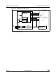

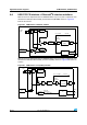
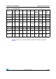
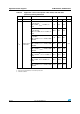


Table Of Contents
- Table 1. Device summary
- 1 Introduction
- 2 Description
- 2.1 Device overview
- 2.2 Full compatibility throughout the family
- 2.3 Overview
- Figure 1. STM32F105xx and STM32F107xx connectivity line block diagram
- 2.3.1 ARM® Cortex™-M3 core with embedded Flash and SRAM
- 2.3.2 Embedded Flash memory
- 2.3.3 CRC (cyclic redundancy check) calculation unit
- 2.3.4 Embedded SRAM
- 2.3.5 Nested vectored interrupt controller (NVIC)
- 2.3.6 External interrupt/event controller (EXTI)
- 2.3.7 Clocks and startup
- 2.3.8 Boot modes
- 2.3.9 Power supply schemes
- 2.3.10 Power supply supervisor
- 2.3.11 Voltage regulator
- 2.3.12 Low-power modes
- 2.3.13 DMA
- 2.3.14 RTC (real-time clock) and backup registers
- 2.3.15 Timers and watchdogs
- 2.3.16 I²C bus
- 2.3.17 Universal synchronous/asynchronous receiver transmitters (USARTs)
- 2.3.18 Serial peripheral interface (SPI)
- 2.3.19 Inter-integrated sound (I2S)
- 2.3.20 Ethernet MAC interface with dedicated DMA and IEEE 1588 support
- 2.3.21 Controller area network (CAN)
- 2.3.22 Universal serial bus on-the-go full-speed (USB OTG FS)
- 2.3.23 GPIOs (general-purpose inputs/outputs)
- 2.3.24 Remap capability
- 2.3.25 ADCs (analog-to-digital converters)
- 2.3.26 DAC (digital-to-analog converter)
- 2.3.27 Temperature sensor
- 2.3.28 Serial wire JTAG debug port (SWJ-DP)
- 2.3.29 Embedded Trace Macrocell™
- 3 Pinouts and pin description
- 4 Memory mapping
- 5 Electrical characteristics
- 5.1 Parameter conditions
- 5.2 Absolute maximum ratings
- 5.3 Operating conditions
- 5.3.1 General operating conditions
- 5.3.2 Operating conditions at power-up / power-down
- 5.3.3 Embedded reset and power control block characteristics
- 5.3.4 Embedded reference voltage
- 5.3.5 Supply current characteristics
- Table 13. Maximum current consumption in Run mode, code with data processing running from Flash
- Table 14. Maximum current consumption in Run mode, code with data processing running from RAM
- Table 15. Maximum current consumption in Sleep mode, code running from Flash or RAM
- Table 16. Typical and maximum current consumptions in Stop and Standby modes
- Figure 10. Typical current consumption on VBAT with RTC on vs. temperature at different VBAT values
- Figure 11. Typical current consumption in Stop mode with regulator in Run mode versus temperature at different VDD values
- Figure 12. Typical current consumption in Stop mode with regulator in Low-power mode versus temperature at different VDD values
- Figure 13. Typical current consumption in Standby mode versus temperature at different VDD values
- Table 17. Typical current consumption in Run mode, code with data processing running from Flash
- Table 18. Typical current consumption in Sleep mode, code running from Flash or RAM
- Table 19. Peripheral current consumption
- 5.3.6 External clock source characteristics
- Table 20. High-speed external user clock characteristics
- Table 21. Low-speed external user clock characteristics
- Figure 14. High-speed external clock source AC timing diagram
- Figure 15. Low-speed external clock source AC timing diagram
- Table 22. HSE 3-25 MHz oscillator characteristics
- Figure 16. Typical application with an 8 MHz crystal
- Table 23. LSE oscillator characteristics (fLSE = 32.768 kHz)
- Figure 17. Typical application with a 32.768 kHz crystal
- 5.3.7 Internal clock source characteristics
- 5.3.8 PLL, PLL2 and PLL3 characteristics
- 5.3.9 Memory characteristics
- 5.3.10 EMC characteristics
- 5.3.11 Absolute maximum ratings (electrical sensitivity)
- 5.3.12 I/O current injection characteristics
- 5.3.13 I/O port characteristics
- Table 36. I/O static characteristics
- Figure 18. Standard I/O input characteristics - CMOS port
- Figure 19. Standard I/O input characteristics - TTL port
- Figure 20. 5 V tolerant I/O input characteristics - CMOS port
- Figure 21. 5 V tolerant I/O input characteristics - TTL port
- Table 37. Output voltage characteristics
- Table 38. I/O AC characteristics
- Figure 22. I/O AC characteristics definition
- 5.3.14 NRST pin characteristics
- 5.3.15 TIM timer characteristics
- 5.3.16 Communications interfaces
- Table 41. I2C characteristics
- Figure 24. I2C bus AC waveforms and measurement circuit
- Table 42. SCL frequency (fPCLK1= 36 MHz.,VDD = 3.3 V)
- Table 43. SPI characteristics
- Figure 25. SPI timing diagram - slave mode and CPHA = 0
- Figure 26. SPI timing diagram - slave mode and CPHA = 1(1)
- Figure 27. SPI timing diagram - master mode(1)
- Table 44. I2S characteristics
- Figure 28. I2S slave timing diagram (Philips protocol)(1)
- Figure 29. I2S master timing diagram (Philips protocol)(1)
- Table 45. USB OTG FS startup time
- Table 46. USB OTG FS DC electrical characteristics
- Figure 30. USB OTG FS timings: definition of data signal rise and fall time
- Table 47. USB OTG FS electrical characteristics
- Table 48. Ethernet DC electrical characteristics
- Figure 31. Ethernet SMI timing diagram
- Table 49. Dynamic characteristics: Ethernet MAC signals for SMI
- Figure 32. Ethernet RMII timing diagram
- Table 50. Dynamic characteristics: Ethernet MAC signals for RMII
- Figure 33. Ethernet MII timing diagram
- Table 51. Dynamic characteristics: Ethernet MAC signals for MII
- 5.3.17 12-bit ADC characteristics
- Table 52. ADC characteristics
- Table 53. RAIN max for fADC = 14 MHz
- Table 54. ADC accuracy - limited test conditions
- Table 55. ADC accuracy
- Figure 34. ADC accuracy characteristics
- Figure 35. Typical connection diagram using the ADC
- Figure 36. Power supply and reference decoupling (VREF+ not connected to VDDA)
- Figure 37. Power supply and reference decoupling (VREF+ connected to VDDA)
- 5.3.18 DAC electrical specifications
- 5.3.19 Temperature sensor characteristics
- 6 Package characteristics
- 6.1 Package mechanical data
- Figure 39. LFBGA100 - 10 x 10 mm low profile fine pitch ball grid array package outline
- Table 58. LFBGA100 - 10 x 10 mm low profile fine pitch ball grid array package mechanical data
- Figure 40. Recommended PCB design rules (0.80/0.75 mm pitch BGA)
- Figure 41. LQFP100, 100-pin low-profile quad flat package outline
- Figure 42. Recommended footprint(1)
- Table 59. LQPF100 – 100-pin low-profile quad flat package mechanical data
- Figure 43. LQFP64 – 64 pin low-profile quad flat package outline
- Figure 44. Recommended footprint(1)
- Table 60. LQFP64 – 64 pin low-profile quad flat package mechanical data
- 6.2 Thermal characteristics
- 6.1 Package mechanical data
- 7 Part numbering
- Appendix A Application block diagrams
- Revision history

STM32F105xx, STM32F107xx
Doc ID 15274 Rev 6 103/103
Please Read Carefully:
Information in this document is provided solely in connection with ST products. STMicroelectronics NV and its subsidiaries (“ST”) reserve the
right to make changes, corrections, modifications or improvements, to this document, and the products and services described herein at any
time, without notice.
All ST products are sold pursuant to ST’s terms and conditions of sale.
Purchasers are solely responsible for the choice, selection and use of the ST products and services described herein, and ST assumes no
liability whatsoever relating to the choice, selection or use of the ST products and services described herein.
No license, express or implied, by estoppel or otherwise, to any intellectual property rights is granted under this document. If any part of this
document refers to any third party products or services it shall not be deemed a license grant by ST for the use of such third party products
or services, or any intellectual property contained therein or considered as a warranty covering the use in any manner whatsoever of such
third party products or services or any intellectual property contained therein.
UNLESS OTHERWISE SET FORTH IN ST’S TERMS AND CONDITIONS OF SALE ST DISCLAIMS ANY EXPRESS OR IMPLIED
WARRANTY WITH RESPECT TO THE USE AND/OR SALE OF ST PRODUCTS INCLUDING WITHOUT LIMITATION IMPLIED
WARRANTIES OF MERCHANTABILITY, FITNESS FOR A PARTICULAR PURPOSE (AND THEIR EQUIVALENTS UNDER THE LAWS
OF ANY JURISDICTION), OR INFRINGEMENT OF ANY PATENT, COPYRIGHT OR OTHER INTELLECTUAL PROPERTY RIGHT.
UNLESS EXPRESSLY APPROVED IN WRITING BY TWO AUTHORIZED ST REPRESENTATIVES, ST PRODUCTS ARE NOT
RECOMMENDED, AUTHORIZED OR WARRANTED FOR USE IN MILITARY, AIR CRAFT, SPACE, LIFE SAVING, OR LIFE SUSTAINING
APPLICATIONS, NOR IN PRODUCTS OR SYSTEMS WHERE FAILURE OR MALFUNCTION MAY RESULT IN PERSONAL INJURY,
DEATH, OR SEVERE PROPERTY OR ENVIRONMENTAL DAMAGE. ST PRODUCTS WHICH ARE NOT SPECIFIED AS "AUTOMOTIVE
GRADE" MAY ONLY BE USED IN AUTOMOTIVE APPLICATIONS AT USER’S OWN RISK.
Resale of ST products with provisions different from the statements and/or technical features set forth in this document shall immediately void
any warranty granted by ST for the ST product or service described herein and shall not create or extend in any manner whatsoever, any
liability of ST.
ST and the ST logo are trademarks or registered trademarks of ST in various countries.
Information in this document supersedes and replaces all information previously supplied.
The ST logo is a registered trademark of STMicroelectronics. All other names are the property of their respective owners.
© 2011 STMicroelectronics - All rights reserved
STMicroelectronics group of companies
Australia - Belgium - Brazil - Canada - China - Czech Republic - Finland - France - Germany - Hong Kong - India - Israel - Italy - Japan -
Malaysia - Malta - Morocco - Philippines - Singapore - Spain - Sweden - Switzerland - United Kingdom - United States of America
www.st.com