
Datasheet


STM32F103xF, STM32F103xG Electrical characteristics
Doc ID 16554 Rev 3 63/120
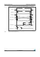
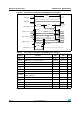
Figure 23. Asynchronous non-multiplexed SRAM/PSRAM/NOR write waveforms
1. Mode 2/B, C and D only. In Mode 1, FSMC_NADV is not used.
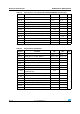
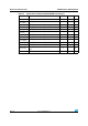
Table 31. Asynchronous non-multiplexed SRAM/PSRAM/NOR read timings
(1)
1. C
L
= 15 pF.
Symbol Parameter Min Max Unit
t
w(NE)
FSMC_NE low time 5t
HCLK
+ 0.5 5t
HCLK
+ 2 ns
t
v(NOE_NE)
FSMC_NEx low to FSMC_NOE low 0.5 1.5 ns
t
w(NOE)
FSMC_NOE low time 5t
HCLK
– 1 5t
HCLK
+ 1 ns
t
h(NE_NOE)
FSMC_NOE high to FSMC_NE high hold time 0 - ns
t
v(A_NE)
FSMC_NEx low to FSMC_A valid - 3 ns
t
h(A_NOE)
Address hold time after FSMC_NOE high 0 - ns
t
v(BL_NE)
FSMC_NEx low to FSMC_BL valid - 0 ns
t
h(BL_NOE)
FSMC_BL hold time after FSMC_NOE high 0.5 - ns
t
su(Data_NE)
Data to FSMC_NEx high setup time 2t
HCLK
- 1 - ns
t
su(Data_NOE)
Data to FSMC_NOEx high setup time 2t
HCLK
- 1 - ns
t
h(Data_NOE)
Data hold time after FSMC_NOE high 0 - ns
t
h(Data_NE)
Data hold time after FSMC_NEx high 0 - ns
t
v(NADV_NE)
FSMC_NEx low to FSMC_NADV low - 0 ns
t
w(NADV)
FSMC_NADV low time - t
HCLK
+ 2 ns
NBL
Data
FSMC_NEx
FSMC_NBL[3:0]
FSMC_D[15:0]
t
v(BL_NE)
t
h(Data_NWE)
FSMC_NOE
Address
FSMC_A[25:0]
t
v(A_NE)
t
w(NWE)
FSMC_NWE
t
v(NWE_NE)
t
h(NE_NWE)
t
h(A_NWE)
t
h(BL_NWE)
t
v(Data_NE)
t
w(NE)
ai14990
FSMC_NADV
(1)
t
v(NADV_NE)
t
w(NADV)