
Datasheet

STM32F103xF, STM32F103xG Electrical characteristics
Doc ID 16554 Rev 3 41/120
5.3 Operating conditions
5.3.1 General operating conditions
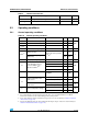
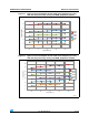
Table 9. Thermal characteristics
Symbol Ratings Value Unit
T
STG
Storage temperature range –65 to +150 °C
T
J
Maximum junction temperature 150 °C
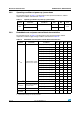
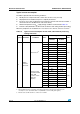
Table 10. General operating conditions
Symbol Parameter Conditions Min Max Unit
f
HCLK
Internal AHB clock frequency 0 72
MHzf
PCLK1
Internal APB1 clock frequency 0 36
f
PCLK2
Internal APB2 clock frequency 0 72
V
DD
Standard operating voltage 2 3.6 V
V
DDA
(1)
1. When the ADC is used, refer to Table 62: ADC characteristics.
Analog operating voltage
(ADC not used)
Must be the same potential
as V
DD
(2)
2. It is recommended to power V
DD
and V
DDA
from the same source. A maximum difference of 300 mV
between V
DD
and V
DDA
can be tolerated during power-up and operation.
23.6
V
Analog operating voltage
(ADC used)
2.4 3.6
V
BAT
Backup operating voltage 1.8 3.6 V
P
D
Power dissipation at T
A
=
85 °C for suffix 6 or T
A
=
105 °C for suffix 7
(3)
3. If T
A
is lower, higher P
D
values are allowed as long as T
J
does not exceed T
J
max (see Table 6.2: Thermal
characteristics on page 114).
LQFP144 - 666
mW
LQFP100 - 434
LQFP64 - 444
LFBGA144 - 500
WLCSP64 - 400
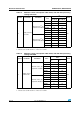
TA
Ambient temperature for 6
suffix version
Maximum power dissipation –40 85
°C
Low power dissipation
(4)
4. In low power dissipation state, T
A
can be extended to this range as long as T
J
does not exceed T
J
max (see
Table 6.2: Thermal characteristics on page 114).
–40 105
Ambient temperature for 7
suffix version
Maximum power dissipation –40 105
°C
Low power dissipation
(4)
–40 125
T
J Junction temperature range
6 suffix version –40 105
°C
7 suffix version –40 125