
Datasheet


Electrical characteristics STM32F103xF, STM32F103xG
40/120 Doc ID 16554 Rev 3
5.2 Absolute maximum ratings
Stresses above the absolute maximum ratings listed in Table 7: Voltage characteristics,
Table 8: Current characteristics, and Tabl e 9: Thermal characteristics may cause permanent
damage to the device. These are stress ratings only and functional operation of the device
at these conditions is not implied. Exposure to maximum rating conditions for extended
periods may affect device reliability.
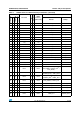
Table 7. Voltage characteristics
Symbol Ratings Min Max Unit
V
DD
–V
SS
External main supply voltage (including V
DDA
and V
DD
)
(1)
1. All main power (V
DD
, V
DDA
) and ground (V
SS
, V
SSA
) pins must always be connected to the external power
supply, in the permitted range.
–0.3 4.0
V
V
IN
(2)
2. V
IN
maximum must always be respected. Refer to Table 8: Current characteristics for the maximum
allowed injected current values.
Input voltage on five volt tolerant pin V
SS
− 0.3 V
DD
+ 4.0
Input voltage on any other pin V
SS
− 0.3 4.0
|ΔV
DDx
| Variations between different V
DD
power pins - 50
mV
|V
SSX
− V
SS
| Variations between all the different ground pins - 50
V
ESD(HBM)
Electrostatic discharge voltage (human body
model)
see Section 5.3.12:
Absolute maximum ratings
(electrical sensitivity)
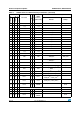
Table 8. Current characteristics
Symbol Ratings Max. Unit
I
VDD
Total current into V
DD
/V
DDA
power lines (source)
(1)
1. All main power (V
DD
, V
DDA
) and ground (V
SS
, V
SSA
) pins must always be connected to the external power
supply, in the permitted range.
150
mA
I
VSS
Total current out of V
SS
ground lines (sink)
(1)
150
I
IO
Output current sunk by any I/O and control pin 25
Output current source by any I/Os and control pin − 25
I
INJ(PIN)
(2)
2. Negative injection disturbs the analog performance of the device. See note 3 below Table 65 on page 103.
Injected current on five volt tolerant pins
(3)
3. Positive injection is not possible on these I/Os. A negative injection is induced by V
IN
<V
SS
. I
INJ(PIN)
must
never be exceeded. Refer to Table 7: Voltage characteristics for the maximum allowed input voltage
values.
-5/+0
Injected current on any other pin
(4)
4. A positive injection is induced by V
IN
>V
DD
while a negative injection is induced by V
IN
<V
SS
. I
INJ(PIN)
must
never be exceeded. Refer to Table 7: Voltage characteristics for the maximum allowed input voltage
values.
± 5
ΣI
INJ(PIN)
Total injected current (sum of all I/O and control pins)
(5)
5. When several inputs are submitted to a current injection, the maximum ΣI
INJ(PIN)
is the absolute sum of the
positive and negative injected currents (instantaneous values).
± 25