
Datasheet

STM32F103xF, STM32F103xG Description
Doc ID 16554 Rev 3 13/120
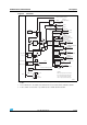
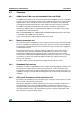
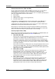
Figure 2. Clock tree
1. When the HSI is used as a PLL clock input, the maximum system clock frequency that can be achieved is
64 MHz.
2. For the USB function to be available, both HSE and PLL must be enabled, with the USBCLK at 48 MHz.
3. To have an ADC conversion time of 1 µs, APB2 must be at 14 MHz, 28 MHz or 56 MHz.
HSE OSC
4-16 MHz
OSC_IN
OSC_OUT
OSC32_IN
OSC32_OUT
LSE OSC
32.768 kHz
HSI RC
8 MHz
LSI RC
40 kHz
to Independent Watchdog (IWDG)
PLL
x2, x3, x4
PLLMUL
HSE = High-speed external clock signal
LSE =
LSI =
HSI =
Legend:
MCO
Clock Output
Main
PLLXTPRE
/2
..., x16
AHB
Prescaler
/1, 2..512
/2
PLLCLK
HSI
HSE
APB1
Prescaler
/1, 2, 4, 8, 16
ADC
Prescaler
/2, 4, 6, 8
ADCCLK
PCLK1
HCLK
PLLCLK
to AHB bus, core,
memory and DMA
USBCLK
to USB interface
USB
Prescaler
/1, 1.5
to ADC1, 2 or 3
LSE
LSI
HSI
/128
/2
HSI
HSE
peripherals
to APB1
Peripheral Clock
Enable
Enable
Peripheral Clock
APB2
Prescaler
/1, 2, 4, 8, 16
PCLK2
TIM1, 8, 9, 10, 11
to TIM1/8
and TIM9/10/11
peripherals to APB2
Peripheral Clock
Enable
Enable
Peripheral Clock
48 MHz
72 MHz max
72 MHz
72 MHz max
36 MHz max
to RTC
PLLSRC
SW
MCO
CSS
to Cortex System timer
/8
Clock
Enable
SYSCLK
max
RTCCLK
RTCSEL[1:0]
TIMxCLK
TIMxCLK
IWDGCLK
SYSCLK
FCLK Cortex
free running clock
/2
TIM2,3,4,5,12,13,14,6,7
to TIM2/3/4/5/12/13/14
and TIM6/7
To SDIO AHB interface
Peripheral clock
enable
HCLK/2
to FSMC
FSMCCLK
to SDIO
Peripheral clock
enable
Peripheral clock
enable
to I2S3
to I2S2
Peripheral clock
enable
Peripheral clock
enable
I2S3CLK
I2S2CLK
SDIOCLK
ai17354
If (APB1 prescaler =1) x1
else x2
If (APB2 prescaler =1) x1
else x2
High-speed internal clock signal
Low-speed internal clock signal
Low-speed external clock signal
FLITFCLK
to Flash programming interface