
Datasheet

STM32F103xF, STM32F103xG Description
Doc ID 16554 Rev 3 11/120
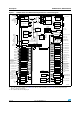
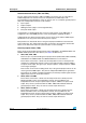
2.1 Device overview
The STM32F103xx XL-density performance line family offers devices in four different
package types: from 64 pins to 144 pins. Depending on the device chosen, different sets of
peripherals are included, the description below gives an overview of the complete range of
peripherals proposed in this family.
Figure 1 shows the general block diagram of the device family.
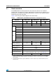
Table 2. STM32F103xF and STM32F103xG features and peripheral counts
Peripherals STM32F103Rx STM32F103Vx STM32F103Zx
Flash memory 768 KB 1 MB 768 KB 1 MB 768 KB 1 MB
SRAM in Kbytes 96 96 96
FSMC No Yes
(1)
1. For the LQFP100 package, only FSMC Bank1 and Bank2 are available. Bank1 can only support a
multiplexed NOR/PSRAM memory using the NE1 Chip Select. Bank2 can only support a 16- or 8-bit NAND
Flash memory using the NCE2 Chip Select. The interrupt line cannot be used since Port G is not available
in this package.
Ye s
Timers
General-purpose 10
Advanced-control 2
Basic 2
Comm
SPI(I
2
S)
(2)
2. The SPI2 and SPI3 interfaces give the flexibility to work in an exclusive way in either the SPI mode or the
I
2
S audio mode.
3(2)
I
2
C2
USART 5
USB 1
CAN 1
SDIO 1
GPIOs 51 80 112
12-bit ADC
Number of channels
3
16
3
16
3
21
12-bit DAC
Number of channels
2
2
CPU frequency 72 MHz
Operating voltage 2.0 to 3.6 V
Operating temperatures
Ambient temperatures: –40 to +85 °C /–40 to +105 °C (see Ta ble 10)
Junction temperature: –40 to + 125 °C (see Table 10)
Package LQFP64 LQFP100 LQFP144, BGA144