
Datasheet

STM32F103xF, STM32F103xG Electrical characteristics
Doc ID 16554 Rev 3 101/120
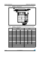
5.3.19 12-bit ADC characteristics
Unless otherwise specified, the parameters given in Ta b l e 62 are preliminary values derived
from tests performed under ambient temperature, f
PCLK2
frequency and V
DDA
supply voltage
conditions summarized in
Ta ble 10.
Note: It is recommended to perform a calibration after each power-up.
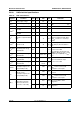
Table 62. ADC characteristics
Symbol Parameter Conditions Min Typ
Max Unit
V
DDA
Power supply 2.4 - 3.6 V
V
REF+
Positive reference voltage 2.4 - V
DDA
V
I
VREF
Current on the V
REF
input
pin
-160220
(1)
µA
f
ADC
ADC clock frequency 0.6 - 14 MHz
f
S
(2)
Sampling rate 0.05 - 1 MHz
f
TRIG
(2)
External trigger frequency
f
ADC
= 14 MHz - - 823 kHz
--171/f
ADC
V
AIN
Conversion voltage range
(3)
0 (V
SSA
or V
REF-
tied to ground)
-V
REF+
V
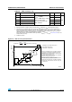
R
AIN
(2)
External input impedance
See Equation 1 and
Table 63 for details
--50kΩ
R
ADC
(2)
Sampling switch resistance - - 1 kΩ
C
ADC
(2)
Internal sample and hold
capacitor
--8pF
t
CAL
(2)
Calibration time
f
ADC
= 14 MHz 5.9 µs
83 1/f
ADC
t
lat
(2)
Injection trigger conversion
latency
f
ADC
= 14 MHz - - 0.214 µs
--3
(4)
1/f
ADC
t
latr
(2)
Regular trigger conversion
latency
f
ADC
= 14 MHz - - 0.143 µs
--2
(4)
1/f
ADC
t
S
(2)
Sampling time
f
ADC
= 14 MHz 0.107 - 17.1 µs
1.5 - 239.5 1/f
ADC
t
STAB
(2)
Power-up time 0 0 1 µs
t
CONV
(2)
Total conversion time
(including sampling time)
f
ADC
= 14 MHz 1 18 µs
14 to 252 (t
S
for sampling +12.5 for
successive approximation)
1/f
ADC
1. Based on characterization, not tested in production.
2. Guaranteed by design, not tested in production.
3. V
REF+
can be internally connected to V
DDA
and V
REF-
can be internally connected to V
SSA
, depending on the package.
Refer to Section 3: Pinouts and pin descriptions for further details.
4. For external triggers, a delay of 1/f
PCLK2
must be added to the latency specified in Table 62.