
Datasheet


STM32F103xC, STM32F103xD, STM32F103xE Description
Doc ID 14611 Rev 8 11/130
2.1 Device overview
The STM32F103xx high-density performance line family offers devices in six different
package types: from 64 pins to 144 pins. Depending on the device chosen, different sets of
peripherals are included, the description below gives an overview of the complete range of
peripherals proposed in this family.
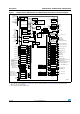
Figure 1 shows the general block diagram of the device family.
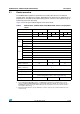
Table 2. STM32F103xC, STM32F103xD and STM32F103xE features and peripheral
counts
Peripherals STM32F103Rx STM32F103Vx STM32F103Zx
Flash memory in Kbytes 256 384 512 256 384 512 256 384 512
SRAM in Kbytes 48 64
(1)
1. 64 KB RAM for 256 KB Flash are available on devices delivered in CSP packages only.
48 64 48 64
FSMC No Yes
(2)
2. For the LQFP100 and BGA100 packages, only FSMC Bank1 and Bank2 are available. Bank1 can only
support a multiplexed NOR/PSRAM memory using the NE1 Chip Select. Bank2 can only support a 16- or
8-bit NAND Flash memory using the NCE2 Chip Select. The interrupt line cannot be used since Port G is
not available in this package.
Ye s
Timers
General-purpose 4
Advanced-control 2
Basic 2
Comm
SPI(I
2
S)
(3)
3. The SPI2 and SPI3 interfaces give the flexibility to work in an exclusive way in either the SPI mode or the
I
2
S audio mode.
3(2)
I
2
C2
USART 5
USB 1
CAN 1
SDIO 1
GPIOs 51 80 112
12-bit ADC
Number of channels
3
16
3
16
3
21
12-bit DAC
Number of channels
2
2
CPU frequency 72 MHz
Operating voltage 2.0 to 3.6 V
Operating temperatures
Ambient temperatures: –40 to +85 °C /–40 to +105 °C (see Ta ble 1 0)
Junction temperature: –40 to + 125 °C (see Tab le 1 0 )
Package LQFP64, WLCSP64 LQFP100, BGA100 LQFP144, BGA144