
Datasheet

Revision history STM32F103x8, STM32F103xB
98/105 DocID13587 Rev 16
18-Oct-2007 3
STM32F103CBT6, STM32F103T6 and STM32F103T8 root part
numbers added (see Table 2: STM32F103xx medium-density device
features and peripheral counts)
VFQFPN36 package added (see Section 6: Package characteristics). All
packages are ECOPACK® compliant. Package mechanical data inch
values are calculated from mm and rounded to 4 decimal digits (see
Section 6: Package characteristics).
Table 5: Medium-density STM32F103xx pin definitions updated and
clarified.
Table 26: Low-power mode wakeup timings updated.
T
A
min corrected in Table 12: Embedded internal reference voltage.
Note 2 added below Table 22: HSE 4-16 MHz oscillator characteristics.
V
ESD(CDM)
value added to Table 32: ESD absolute maximum ratings.
Note 4 added and V
OH
parameter description modified in Table 36:
Output voltage characteristics.
Note 1 modified under Table 37: I/O AC characteristics.
Equation 1 and Table 47: RAIN max for fADC = 14 MHz added to
Section 5.3.18: 12-bit ADC characteristics.
V
AIN
, t
S
max, t
CONV
, V
REF+
min and t
lat
max modified, notes modified
and t
latr
added in Table 46: ADC characteristics.
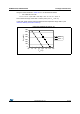
Figure 37: ADC accuracy characteristics updated. Note 1 modified
below Figure 38: Typical connection diagram using the ADC.
Electrostatic discharge (ESD) on page 60 modified.
Number of TIM4 channels modified in Figure 1: STM32F103xx
performance line block diagram.
Maximum current consumption Table 13, Table 14 and Tab le 15
updated. V
hys
modified in Table 35: I/O static characteristics.
Table 49: ADC accuracy updated. t
VDD
modified in Table 10: Operating
conditions at power-up / power-down. V
FESD
value added in Table 30:
EMS characteristics.
Values corrected, note 2 modified and note 3 removed in Table 26: Low-
power mode wakeup timings.
Table 16: Typical and maximum current consumptions in Stop and
Standby modes: Typical values added for V
DD
/V
BAT
= 2.4 V, Note 2
modified, Note 2 added.
Table 21: Typical current consumption in Standby mode added. On-chip
peripheral current consumption on page 50 added.
ACC
HSI
values updated in Table 24: HSI oscillator characteristics.
V
prog
added to Table 28: Flash memory characteristics.
Upper option byte address modified in Figure 11: Memory map.
Typical f
LSI
value added in Table 25: LSI oscillator characteristics and
internal RC value corrected from 32 to 40 kHz in entire document.
T
S_temp
added to Table 50: TS characteristics. N
END
modified in
Table 29: Flash memory endurance and data retention.
T
S_vrefint
added to Table 12: Embedded internal reference voltage.
Handling of unused pins specified in General input/output characteristics
on page 62. All I/Os are CMOS and TTL compliant. Figure 39: Power
supply and reference decoupling (VREF+ not connected to VDDA)
modified.
t
JITTER
and f
VCO
removed from Table 27: PLL characteristics.
Appendix A: Important notes on page 81 added.
Added Figure 16, Figure 17, Figure 19 and Figure 21.
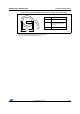
Table 61. Document revision history (continued)
Date Revision Changes