
Datasheet

DocID13587 Rev 16 97/105
STM32F103x8, STM32F103xB Revision history
104
8 Revision history
Table 61. Document revision history
Date Revision Changes
01-jun-2007 1 Initial release.
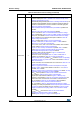
20-Jul-2007 2
Flash memory size modified in Note 9, Note 5, Note 7, Note 7 and
BGA100 pins added to Table 5: Medium-density STM32F103xx pin
definitions. Figure 3: STM32F103xx performance line LFBGA100 ballout
added.
T
HSE
changed to T
LSE
in Figure 23: Low-speed external clock source
AC timing diagram. V
BAT
ranged modified in Power supply schemes.
t
SU(LSE)
changed to t
SU(HSE)
in Table 22: HSE 4-16 MHz oscillator
characteristics. I
DD(HSI)
max value added to Table 24: HSI oscillator
characteristics.
Sample size modified and machine model removed in Electrostatic
discharge (ESD).
Number of parts modified and standard reference updated in Static
latch-up. 25 °C and 85 °C conditions removed and class name modified
in Table 33: Electrical sensitivities. R
PU
and R
PD
min and max values
added to Table 35: I/O static characteristics. R
PU
min and max values
added to Table 38: NRST pin characteristics.
Figure 32: I2C bus AC waveforms and measurement circuit and
Figure 31: Recommended NRST pin protection corrected.
Notes removed below Tabl e 9 , Tabl e 38, Table 44.
I
DD
typical values changed in Table 11: Maximum current consumption
in Run and Sleep modes. Table 39: TIMx characteristics modified.
t
STAB
, V
REF+
value, t
lat
and f
TRIG
added to Table 46: ADC
characteristics.
In Table 29: Flash memory endurance and data retention, typical
endurance and data retention for T
A
= 85 °C added, data retention for T
A
= 25 °C removed.
V
BG
changed to V
REFINT
in Table 12: Embedded internal reference
voltage. Document title changed. Controller area network (CAN) section
modified.
Figure 14: Power supply scheme modified.
Features on page 1 list optimized. Small text changes.