
Datasheet


DocID13587 Rev 16 83/105
STM32F103x8, STM32F103xB Package characteristics
104
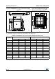
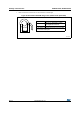
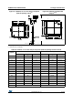
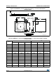
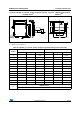
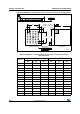
Figure 43. UFQFPN48 7 x 7 mm, 0.5 mm pitch, package outline
1. Drawing is not to scale.
2. There is an exposed die pad on the underside of the QFPN package, this pad is not internally connected to
the VSS or VDD power pads. It is recommended to connect it to VSS.
3. All leads/pads should also be soldered to the PCB to improve the lead solder joint life.
A0B9_ME_V3
D
Pin 1 indentifier
laser marking area
EE
D
Y
D2
E2
Exposed pad
area
Z
1
48
Detail Z
R 0.125 typ.
1
48
L
C 0.500x45°
pin1 corner
A
Seating
plane
A1
b
e
ddd
Detail Y
T
Table 52. UFQFPN48 7 x 7 mm, 0.5 mm pitch, package mechanical data
Symbol
millimeters inches
(1)
Min Typ Max Min Typ Max
A 0.500 0.550 0.600 0.0197 0.0217 0.0236
A1 0.000 0.020 0.050 0.0000 0.0008 0.0020
D 6.900 7.000 7.100 0.2717 0.2756 0.2795
E 6.900 7.000 7.100 0.2717 0.2756 0.2795
D2 5.500 5.600 5.700 0.2165 0.2205 0.2244
E2 5.500 5.600 5.700 0.2165 0.2205 0.2244
L 0.300 0.400 0.500 0.0118 0.0157 0.0197
T - 0.152 - - 0.0060 -