
Datasheet

DocID13587 Rev 16 79/105
STM32F103x8, STM32F103xB Electrical characteristics
104
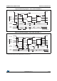
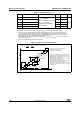
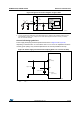
Figure 38. Typical connection diagram using the ADC
1. Refer to Table 46 for the values of R
AIN
, R
ADC
and C
ADC
.
2. C
parasitic
represents the capacitance of the PCB (dependent on soldering and PCB layout quality) plus the
pad capacitance (roughly 7 pF). A high C
parasitic
value will downgrade conversion accuracy. To remedy
this, f
ADC
should be reduced.
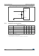
General PCB design guidelines
Power supply decoupling should be performed as shown in Figure 39 or Figure 40,
depending on whether V
REF+
is connected to V
DDA
or not. The 10 nF capacitors should be
ceramic (good quality). They should be placed them as close as possible to the chip.
Figure 39. Power supply and reference decoupling (V
REF+
not connected to V
DDA
)
1. V
REF+
and V
REF–
inputs are available only on 100-pin packages.
ai14150c
STM32F103xx
V
DD
AINx
I
L
±1 µA
0.6 V
V
T
R
AIN
(1)
C
parasitic
V
AIN
0.6 V
V
T
R
ADC
(1)
12-bit
converter
C
ADC
(1)
Sample and hold ADC
converter
V
REF+
(see note 1)
STM32F103xx
V
DDA
V
SSA
/V
REF–
(see note 1)
1 µF // 10 nF
1 µF // 10 nF
ai14388b