
Datasheet

DocID13587 Rev 16 75/105
STM32F103x8, STM32F103xB Electrical characteristics
104
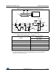
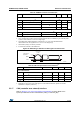
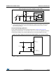
Figure 36. USB timings: definition of data signal rise and fall time
5.3.17 CAN (controller area network) interface
Refer to Section 5.3.12: I/O current injection characteristics for more details on the
input/output alternate function characteristics (CAN_TX and CAN_RX).
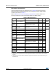
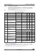
Table 44. USB DC electrical characteristics
Symbol Parameter Conditions Min.
(1)
1. All the voltages are measured from the local ground potential.
Max.
(1)
Unit
Input levels
V
DD
USB operating voltage
(2)
2. To be compliant with the USB 2.0 full-speed electrical specification, the USBDP (D+) pin should be pulled
up with a 1.5 k resistor to a 3.0-to-3.6 V voltage range.
3.0
(3)
3. The STM32F103xx USB functionality is ensured down to 2.7 V but not the full USB electrical
characteristics which are degraded in the 2.7-to-3.0 V V
DD
voltage range.
3.6 V
V
DI
(4)
4. Guaranteed by design, not tested in production.
Differential input sensitivity I(USBDP, USBDM) 0.2 -
VV
CM
(4)
Differential common mode range Includes V
DI
range 0.8 2.5
V
SE
(4)
Single ended receiver threshold 1.3 2.0
Output levels
V
OL
Static output level low R
L
of 1.5 k to 3.6 V
(5)
5.
R
L
is the load connected on the USB drivers
-0.3
V
V
OH
Static output level high R
L
of 15 k to V
SS
(5)
2.8 3.6
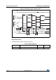
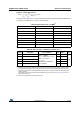
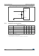
Table 45. USB: Full-speed electrical characteristics
(1)
1. Guaranteed by design, not tested in production.
Symbol Parameter Conditions Min Max Unit
Driver characteristics
t
r
Rise time
(2)
2.
Measured from 10% to 90% of the data signal. For more detailed informations, please refer to USB
Specification - Chapter 7 (version 2.0).
C
L
= 50 pF
420ns
t
f
Fall time
(2)
C
L
= 50 pF 4 20 ns
t
rfm
Rise/ fall time matching t
r
/t
f
90 110 %
V
CRS
Output signal crossover voltage 1.3 2.0 V
ai14137
t
f
Differen tial
data lines
V
SS
V
CR S
t
r
Crossover
points