
Datasheet

Electrical characteristics STM32F103x8, STM32F103xB
72/105 DocID13587 Rev 16
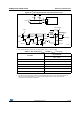
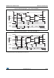
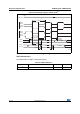
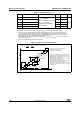
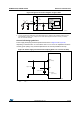
SPI interface characteristics
Unless otherwise specified, the parameters given in Table 42 are derived from tests
performed under the ambient temperature, f
PCLKx
frequency and V
DD
supply voltage
conditions summarized in Table 9.
Refer to Section 5.3.12: I/O current injection characteristics for more details on the
input/output alternate function characteristics (NSS, SCK, MOSI, MISO).
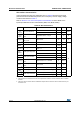
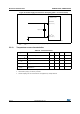
Table 42. SPI characteristics
Symbol Parameter Conditions Min Max Unit
f
SCK
1/t
c(SCK)
SPI clock frequency
Master mode - 18
MHz
Slave mode - 18
t
r(SCK)
t
f(SCK)
SPI clock rise and fall
time
Capacitive load: C = 30 pF - 8 ns
DuCy(SCK)
SPI slave input clock
duty cycle
Slave mode 30 70 %
t
su(NSS)
(1)
1. Based on characterization, not tested in production.
NSS setup time Slave mode 4t
PCLK
-
ns
t
h(NSS)
(1)
NSS hold time Slave mode 2t
PCLK
-
t
w(SCKH)
(1)
t
w(SCKL)
(1)
SCK high and low time
Master mode, f
PCLK
= 36 MHz,
presc = 4
50 60
t
su(MI)
(1)
t
su(SI)
(1)
Data input setup time
Master mode 5 -
Slave mode 5 -
t
h(MI)
(1)
Data input hold time
Master mode 5 -
t
h(SI)
(1)
Slave mode 4 -
t
a(SO)
(1)(2)
2. Min time is for the minimum time to drive the output and the max time is for the maximum time to validate
the data.
Data output access
time
Slave mode, f
PCLK
= 20 MHz 0 3t
PCLK
t
dis(SO)
(1)(3)
3. Min time is for the minimum time to invalidate the output and the max time is for the maximum time to put
the data in Hi-Z
Data output disable
time
Slave mode 2 10
t
v(SO)
(1)
Data output valid time Slave mode (after enable edge) 25
t
v(MO)
(1)
Data output valid time Master mode (after enable edge) 5
t
h(SO)
(1)
Data output hold time
Slave mode (after enable edge) 15 -
t
h(MO)
(1)
Master mode (after enable edge) 2 -