
Datasheet

Electrical characteristics STM32F103xF, STM32F103xG
50/120 Doc ID 16554 Rev 3
Typical current consumption
The MCU is placed under the following conditions:
● All I/O pins are in input mode with a static value at V
DD
or V
SS
(no load).
● All peripherals are disabled except if it is explicitly mentioned.
● The Flash access time is adjusted to f
HCLK
frequency (0 wait state from 0 to 24 MHz, 1
wait state from 24 to 48 MHZ and 2 wait states above).
● Ambient temperature and V
DD
supply voltage conditions summarized in Table 10.
● Prefetch is ON (Reminder: this bit must be set before clock setting and bus prescaling)
When the peripherals are enabled f
PCLK1
= f
HCLK
/4, f
PCLK
2 = f
HCLK
/2, f
ADCCLK
= f
PCLK2
/4
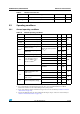
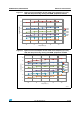
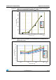
Table 18. Typical current consumption in Run mode, code with data processing
running from Flash
Symbol Parameter Conditions f
HCLK
Typ
(1)
1. Typical values are measures at T
A
= 25 °C, V
DD
= 3.3 V.
Unit
All peripherals
enabled
(2)
2. Add an additional power consumption of 0.8 mA per ADC for the analog part. In applications, this
consumption occurs only while the ADC is on (ADON bit is set in the ADC_CR2 register).
All peripherals
disabled
I
DD
Supply
current in
Run mode
External clock
(3)
3. External clock is 8 MHz and PLL is on when f
HCLK
> 8 MHz.
72 MHz 52.5 33.5
mA
48 MHz 36.6 23.8
36 MHz 28.5 18.7
24 MHz 24.1 12.8
16 MHz 14 9.2
8 MHz 7.7 5.4
4 MHz 4.6 3.4
2 MHz 3 2.3
1 MHz 2.2 1.8
500 kHz 1.7 1.5
125 kHz 1.4 1.3
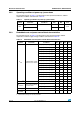
Running on high
speed internal RC
(HSI), AHB
prescaler used to
reduce the
frequency
64 MHz 45.5 28.6
mA
48 MHz 35.1 22.4
36 MHz 27.5 17.5
24 MHz 18.9 11.6
16 MHz 12.2 8.2
8 MHz 7.2 4.8
4 MHz 4 2.7
2 MHz 2.3 1.7
1 MHz 1.5 1.2
500 kHz 1.1 0.9
125 kHz 0.75 0.7