
Datasheet


STM32F103xC, STM32F103xD, STM32F103xE Electrical characteristics
Doc ID 14611 Rev 8 93/130
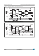
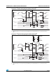
5.3.17 Communications interfaces
I
2
C interface
characteristics
Unless otherwise specified, the parameters given in Ta ble 51 are derived from tests
performed under ambient temperature, f
PCLK1
frequency and V
DD
supply voltage conditions
summarized in Table 1 0 .
The STM32F103xC, STM32F103xD and STM32F103xESTM32F103xF and STM32F103xG
performance line
I
2
C interface meets the requirements of the standard I
2
C communication
protocol with the following restrictions: the I/O pins SDA and SCL are mapped to are not
“true” open-drain. When configured as open-drain, the PMOS connected between the I/O
pin and V
DD
is disabled, but is still present.
The I
2
C characteristics are described in Ta bl e 5 1. Refer also to
Section 5.3.14: I/O port
characteristics
for more details on the input/output alternate function characteristics (SDA
and SCL)
.
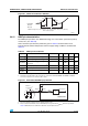
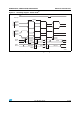
Table 51. I
2
C characteristics
Symbol Parameter
Standard mode I
2
C
(1)
1.
Guaranteed by design, not tested in production.
Fast mode I
2
C
(1)(2)
2. f
PCLK1
must be higher than 2 MHz to achieve standard mode I
2
C frequencies. It must be higher than 4 MHz
to achieve the fast mode I
2
C frequencies and it must be a multiple of 10 MHz in order to reach the I2C fast
mode maximum clock speed of 400 kHz.
Unit
Min Max Min Max
t
w(SCLL)
SCL clock low time 4.7 1.3
µs
t
w(SCLH)
SCL clock high time 4.0 0.6
t
su(SDA)
SDA setup time 250 100
ns
t
h(SDA)
SDA data hold time 0
(3)
3.
The maximum hold time of the Start condition has only to be met if the interface does not stretch the low
period of SCL signal.
0
(4)
4.
The device must internally provide a hold time of at least 300ns for the SDA signal in order to bridge the
undefined region of the falling edge of SCL.
900
(3)
t
r(SDA)
t
r(SCL)
SDA and SCL rise time 1000 20 + 0.1C
b
300
t
f(SDA)
t
f(SCL)
SDA and SCL fall time 300 300
t
h(STA)
Start condition hold time 4.0 0.6
µs
t
su(STA)
Repeated Start condition
setup time
4.7 0.6
t
su(STO)
Stop condition setup time 4.0 0.6 μs
t
w(STO:STA)
Stop to Start condition time
(bus free)
4.7 1.3 μs
C
b
Capacitive load for each bus
line
400 400 pF