
Datasheet

STM32F103xC, STM32F103xD, STM32F103xE Description
Doc ID 14611 Rev 8 17/130
2.3.10 Boot modes
At startup, boot pins are used to select one of three boot options:
● Boot from user Flash: you have an option to boot from any of two memory banks. By
default, boot from Flash memory bank 1 is selected. You can choose to boot from Flash
memory bank 2 by setting a bit in the option bytes.
● Boot from system memory
● Boot from embedded SRAM
The boot loader is located in system memory. It is used to reprogram the Flash memory by
using USART1.
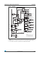
2.3.11 Power supply schemes
● V
DD
= 2.0 to 3.6 V: external power supply for I/Os and the internal regulator.
Provided externally through V
DD
pins.
● V
SSA
, V
DDA
= 2.0 to 3.6 V: external analog power supplies for ADC, DAC, Reset blocks,
RCs and PLL (minimum voltage to be applied to VDDA is 2.4 V when the ADC or DAC
is used). V
DDA
and V
SSA
must be connected to V
DD
and V
SS
, respectively.
● V
BAT
= 1.8 to 3.6 V: power supply for RTC, external clock 32 kHz oscillator and backup
registers (through power switch) when V
DD
is not present.
For more details on how to connect power pins, refer to Figure 12: Power supply scheme.
2.3.12 Power supply supervisor
The device has an integrated power-on reset (POR)/power-down reset (PDR) circuitry. It is
always active, and ensures proper operation starting from/down to 2 V. The device remains
in reset mode when V
DD
is below a specified threshold, V
POR/PDR
, without the need for an
external reset circuit.
The device features an embedded programmable voltage detector (PVD) that monitors the
V
DD
/V
DDA
power supply and compares it to the V
PVD
threshold. An interrupt can be
generated when V
DD
/V
DDA
drops below the V
PVD
threshold and/or when V
DD
/V
DDA
is higher
than the V
PVD
threshold. The interrupt service routine can then generate a warning
message and/or put the MCU into a safe state. The PVD is enabled by software. Refer to
Table 12: Embedded reset and power control block characteristics for the values of
V
POR/PDR
and V
PVD
.
2.3.13 Voltage regulator
The regulator has three operation modes: main (MR), low power (LPR) and power down.
● MR is used in the nominal regulation mode (Run)
● LPR is used in the Stop modes.
● Power down is used in Standby mode: the regulator output is in high impedance: the
kernel circuitry is powered down, inducing zero consumption (but the contents of the
registers and SRAM are lost)
This regulator is always enabled after reset. It is disabled in Standby mode.