
Datasheet


STM32F103xC, STM32F103xD, STM32F103xE Revision history
Doc ID 14611 Rev 8 127/130
30-Mar-2009 5
I/O information clarified on page 1. Figure 4: STM32F103xC and
STM32F103xE performance line BGA100 ballout corrected.
I/O information clarified on page 1.
In Table 5: High-density STM32F103xx pin definitions:
– I/O level of pins PF11, PF12, PF13, PF14, PF15, G0, G1 and G15
updated
– PB4, PB13, PB14, PB15, PB3/TRACESWO moved from Default
column to Remap column
PG14 pin description modified in Table 6: FSMC pin definition.
Figure 9: Memory map on page 38 modified.
Note modified in Table 14: Maximum current consumption in Run mode,
code with data processing running from Flash and Table 16: Maximum
current consumption in Sleep mode, code running from Flash or RAM.
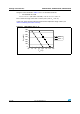
Figure 17, Figure 18 and Figure 19 show typical curves (titles
changed).
Table 21: High-speed external user clock characteristics and Ta bl e 22:
Low-speed external user clock characteristics modified. ACC
HSI
max
values modified in Table 25: HSI oscillator characteristics.
FSMC configuration modified for Asynchronous waveforms and timings.
Notes modified below Figure 24: Asynchronous non-multiplexed
SRAM/PSRAM/NOR read waveforms and Figure 25: Asynchronous
non-multiplexed SRAM/PSRAM/NOR write waveforms.
t
w(NADV)
values modified in Table 31: Asynchronous non-multiplexed
SRAM/PSRAM/NOR read timings
and Table 34: Asynchronous
multiplexed PSRAM/NOR write timings. t
h(Data_NWE)
modified in
Table 32: Asynchronous non-multiplexed SRAM/PSRAM/NOR write
timings
In Table 36: Synchronous multiplexed PSRAM write timings and
Table 38: Synchronous non-multiplexed PSRAM write timings:
–t
v(Data-CLK)
renamed as t
d(CLKL-Data)
–t
d(CLKL-Data)
min value removed and max value added
–t
h(CLKL-DV)
/ t
h(CLKL-ADV)
removed
Figure 28: Synchronous multiplexed NOR/PSRAM read timings,
Figure 29: Synchronous multiplexed PSRAM write timings and
Figure 31: Synchronous non-multiplexed PSRAM write timings
modified.
Figure 52: I2S slave timing diagram (Philips protocol)(1) and Figure 53:
I2S master timing diagram (Philips protocol)(1) modified.
WLCSP64 package added (see Figure 8: STM32F103xC and
STM32F103xE performance line WLCSP64 ballout, ball side, Tab l e 5 :
High-density STM32F103xx pin definitions, Figure 65: WLCSP, 64-ball
4.466 × 4.395 mm, 0.500 mm pitch, wafer-level chip-scale package
outline and Table 68: WLCSP, 64-ball 4.466 × 4.395 mm, 0.500 mm
pitch, wafer-level chip-scale package mechanical data).
Small text changes.
Table 75. Document revision history
Date Revision Changes